Why SEM Lab’s Evidence Driven Analysis is Different from Generic AI
Turning Real Failure Investigations into Actionable Engineering Insight
March 12 2026
Executive Overview
Many organizations now use artificial intelligence tools to obtain technical explanations or summaries. While these tools can provide useful background knowledge, they generally rely on broad training data drawn from textbooks, public documents, and online sources. SEM Lab’s analytical system operates differently. Instead of generating answers from general information, it derives conclusions directly from a large archive of real engineering investigations. This archive contains failure analyses, materials examinations, and microscopy-based studies conducted on electronic assemblies and components across many industries.
Generic AI: Knowledge from Public Sources
Conventional AI systems are trained on large collections of public text. When asked about a technical topic, these systems generate answers based on patterns learned from those materials. This approach can provide reasonable explanations of common engineering concepts. However, the answers are typically generalized and may not reflect the specific conditions present in a client’s manufacturing environment, materials system, or product design. In practical terms, generic AI tools can explain what usually happens in theory, but they cannot reference the specific failures that have occurred in a particular organization or product line.
SEM Lab’s Approach: Evidence from Real Investigations
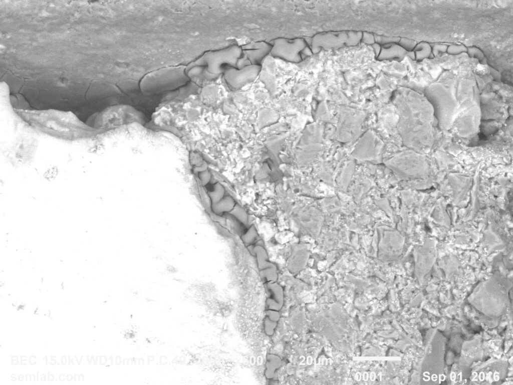
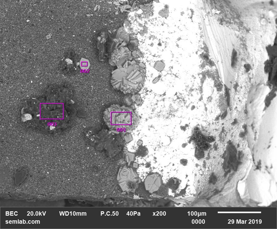
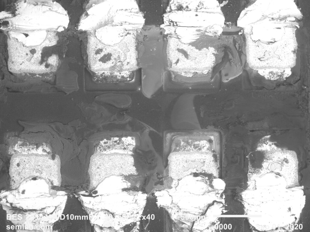
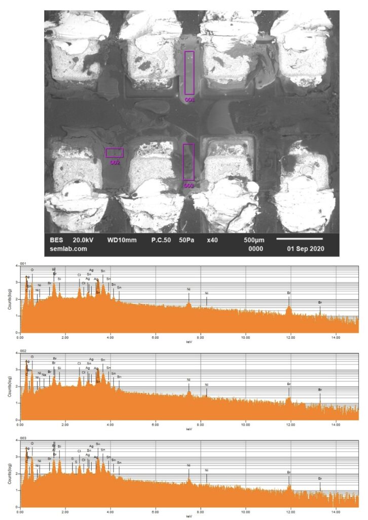
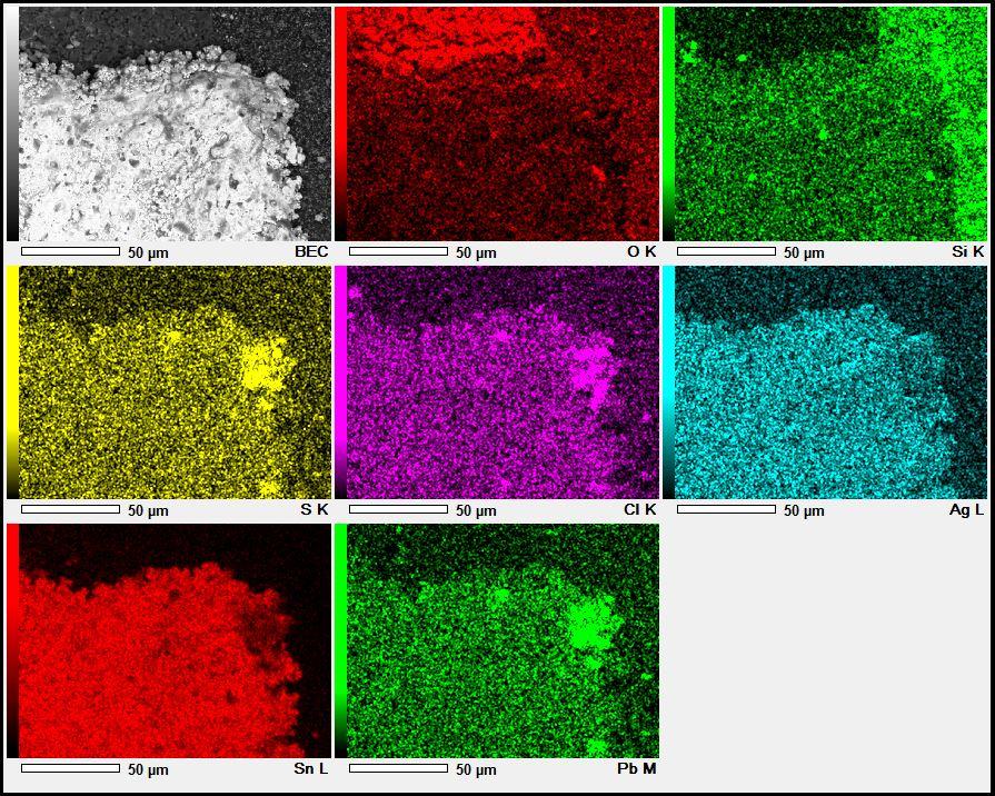
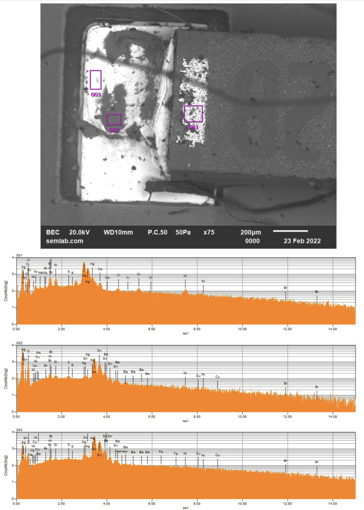
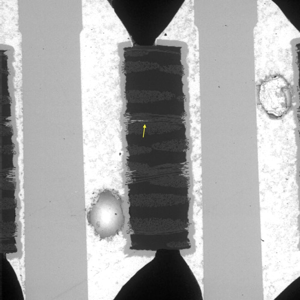
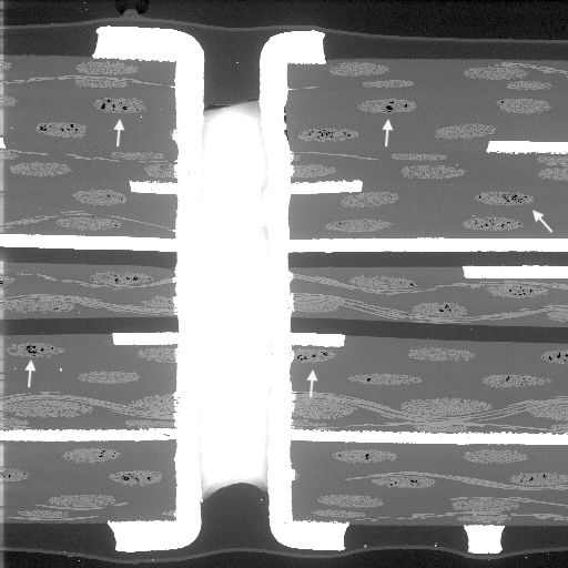
SEM Lab applies a different model. Instead of relying on general knowledge alone, the system analyzes the historical record of failure investigations performed by the laboratory. These investigations include microscopy analysis, materials characterization, contamination studies, fracture analysis, and root cause determination. Each report contributes technical observations that become part of a structured engineering knowledge base. When a topic is analyzed—such as capacitor cracking, flux contamination, or metallization corrosion—the system identifies the real investigations in which those phenomena occurred. The resulting explanation is therefore grounded in documented engineering evidence.
Traceable Engineering Evidence
One of the key advantages of the SEM Lab approach is traceability. Conclusions are supported by identifiable investigations, analytical observations, and materials evidence. Instead of producing a purely narrative explanation, the system can show: • the investigations where the failure mechanism occurred • the materials and components involved • the analytical techniques used to identify the mechanism • the environmental or manufacturing conditions associated with the failure This allows engineering teams to move beyond general explanations toward evidence supported conclusions.
Why This Matters to Manufacturers
Manufacturing and reliability problems rarely arise from generic causes alone. They are usually the result of specific combinations of materials, process conditions, and environmental exposure. Because SEM Lab’s knowledge base is derived from real investigations, it captures the subtle interactions that often drive these failures. These insights help organizations understand not only what failed, but why the failure occurred in their system. This capability allows SEM Lab to provide targeted guidance on issues such as contamination control, assembly process design, materials compatibility, and reliability improvement.
Consulting Applications
The analytical framework behind the SEM Lab knowledge system supports a wide range of consulting services. These include engineering support for: • root cause investigation of field failures • contamination and corrosion analysis • electronic assembly reliability assessments • materials compatibility evaluation • process improvement for soldering and assembly operations by combining laboratory investigation with evidence driven knowledge extraction, SEM Lab can provide engineering recommendations grounded in real-world failure data.
Conclusion
Artificial intelligence tools are becoming widely available, but their usefulness depends on the data and engineering insight that support them. Generic AI systems provide broad explanations derived from public information. SEM Lab’s system, by contrast, extracts knowledge from decades of failure analysis investigations. The resulting insights are not theoretical descriptions—they are reflections of real failures observed in electronic systems. For organizations seeking to understand complex reliability problems, this evidence-based approach provides a stronger foundation for technical decisions and corrective action.
Contact: Ed Hare – SEM Lab, Inc. – Consulting
email: ehare@semlab.com