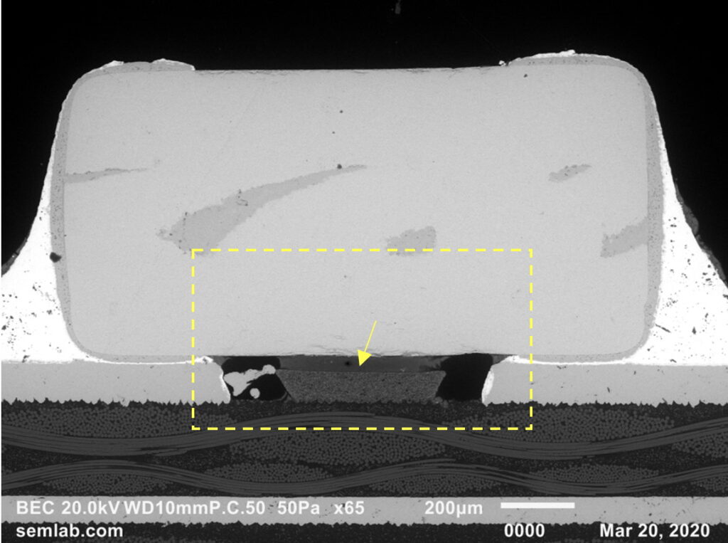
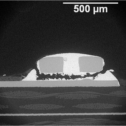
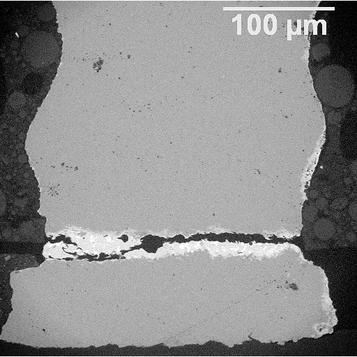
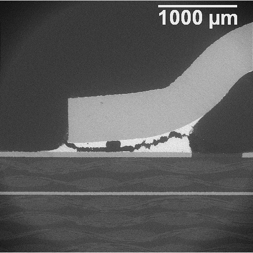
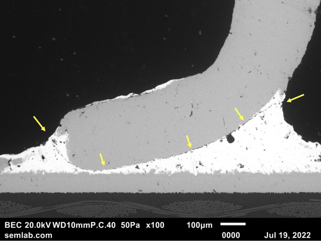
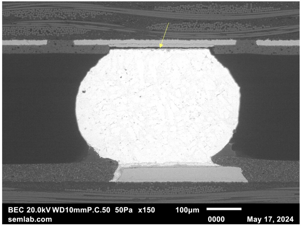
In multilayer printed wiring boards (PWBs), internal shorts can arise from subtle but critical manufacturing defects. This case study highlights a failure mode linked to drill or inner layer misregistration, which compromised the electrical clearance between a plated through-hole (PTH) via and a 24V internal plane. The resulting drill-induced laminate damage, combined with radial cracking, facilitated an unintended electrical bridge. Through microsectional and optical analysis, we demonstrate how mechanical misalignments propagate into latent electrical reliability risks.
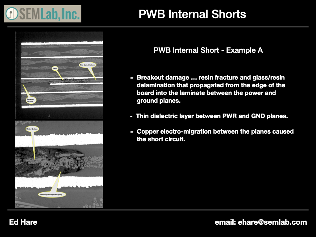
Power and ground plane shorts in multilayer PCBs can be difficult to trace, especially when the root cause lies deep within the laminate structure. This example highlights an internal short caused by resin fracture and delamination, which enabled copper electro-migration across a thin dielectric layer. Understanding failure mechanisms like this is essential for improving PCB reliability in demanding applications. #FailureAnalysis #PCBDesign #ElectroMigration #MaterialsScience
MLCC short circuit failures on PCBAs are often caused by bending fractures, where internal electromigration shorts develop between opposite electrodes along the fracture. Short circuit failures are also caused sometimes by capacitor manufacturing defects such as knit line failure, firing cracks, or dielectric porosity. But we see more frequently in recent years cases where the capacitor short is external, growing due to electrochemical migration through flux entrapped under the MLCC from terminal to terminal.
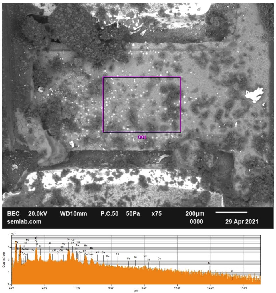
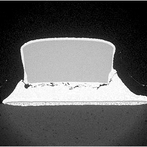
Fortunately, our primary method of examination of MLCCs is a microsection of the capacitor as mounted on the PCBA (Fig. A). This orientation is ideal for evaluation of bending fractures. It also affords us a look under the capacitor.
Fig. A – MLCC microsection as mounted on the PCBA.
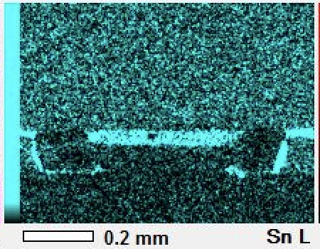
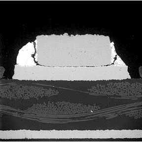
An EDS map for Sn (Fig. B) shows a large concentration of tin below the capacitor and above the solder mask. This indicates that an electrochemical cell existed under the capacitor allowing tin to migrate from the anode to the cathode. The PCBA was operating in a moist environment, which is a contributing factor.
Fig. B – EDS map for tin corresponding with Fig. A dashed box.
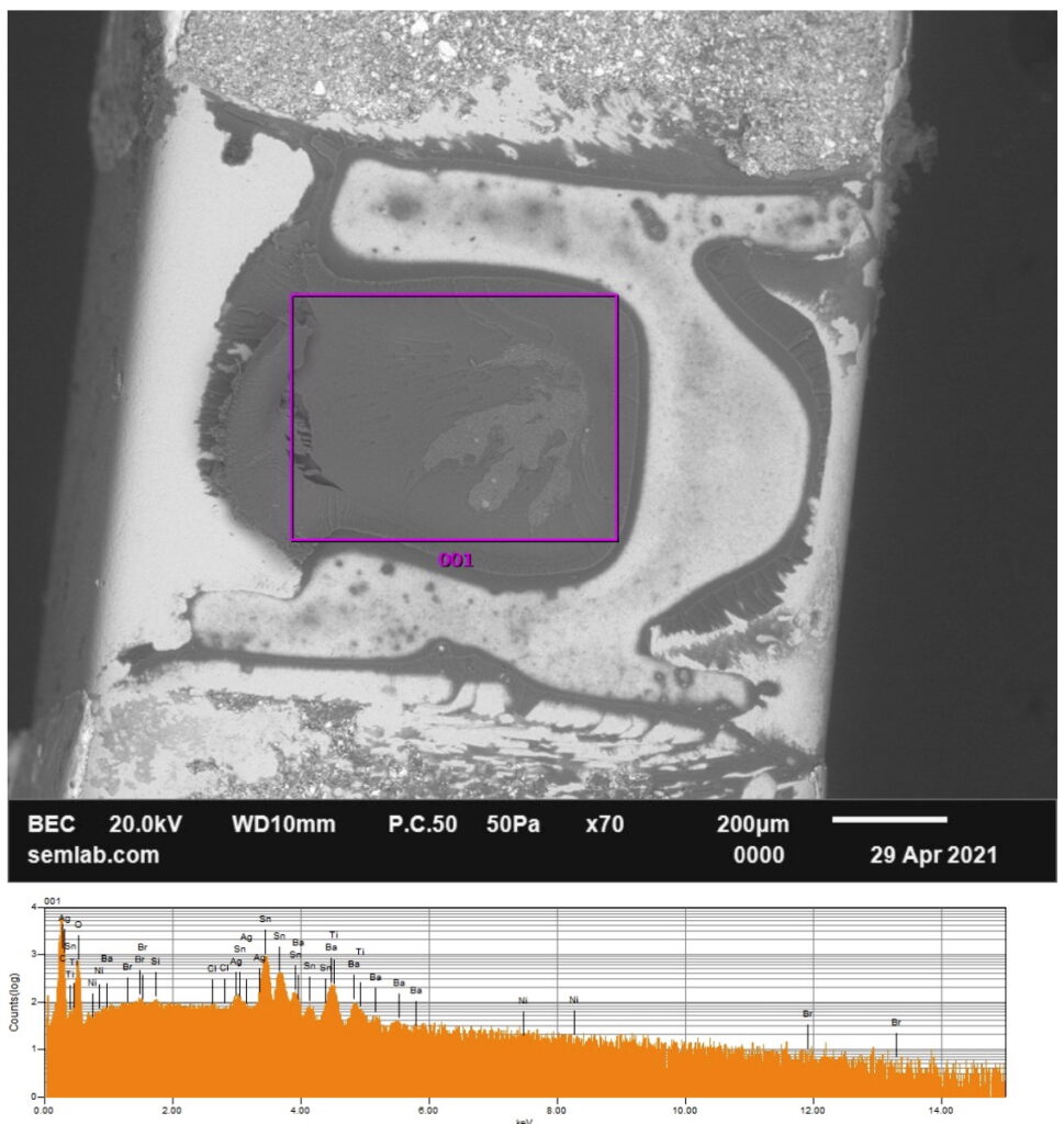
A second way we can look at the problem is to mechanically excavate the solder joints and remove the capacitor from the PCBA so that residue and corrosion damage can be observed on the board surface under the capacitor (Fig. C) and on the bottom surface of the capacitor (Fig. D).
Fig. C – Corrosion damage on the board surface under the capacitor.
Fig. D – Corrosion damage on the bottom surface of the capacitor.
Electrochemical corrosion and electromigration can involve more than corrosion of tin, as we also see corrosion of silver, copper, and nickel plating associated with metal end caps and PWB mounting pads or from SAC305 solder.
Contamination by chlorine and bromine flux activators is common and accelerates the rate of corrosion.
This is how it works …
Residual solder flux absorbs moisture from the environment, creating an ionic solution under the MLCC.
Under applied voltage, metals such as silver (Ag), tin (Sn), nickel (Ni) or copper (Cu) from electrodes or solder pads ionize.
Metal cations migrate toward the cathode.
At the cathode, metal ions are reduced and deposited as metallic dendrites.
Dendrites grow until they bridge the gap between electrodes, creating a short circuit.
Even if the corrosion process doesn’t create a hard metallic short, the generation of ionic species under the capacitor can cause large enough leakage currents to generate circuit faults.
Time to failure is a function of many parameters including quantity and type of solder flux residues, operating temperature, moisture level, and electric field magnitude. The electric field becomes a significant factor as capacitor size decreases. As MLCC sizes decrease, the gap between electrodes (spacing under the component) also shrinks so that the electric field is higher.
So my question to circuit designers is …
How do you incorporate these considerations into your design rules?
These images show the various types of fractures affecting solder joints in electronic assemblies, which includes mechanical overload failures, thermal fatigue due to coefficient of thermal expansion (CTE) mismatches, gold embrittlement, creep rupture failures, and vibration fatigue fractures. Understanding these failure modes is crucial for enhancing the reliability and performance of electronic components.
BGA solder joint failed due to high-strain-rate bending of the PCBA
The relationship between PCBA bending and failures is critical, as bending stresses introduced during manufacturing, assembly, or operation can lead to a wide range of failures, including cracks, fractures, and deformations. These failures often occur in solder joints, component leads, and critical connection points, compromising the reliability and durability of the assemblies. Key mitigation strategies include robust design practices such as incorporating stiffeners, careful material selection to withstand mechanical stresses, controlled manufacturing processes to minimize stress introduction, and careful handling procedures. Understanding and addressing these factors through targeted improvements can significantly reduce bending-related failures, ensuring more reliable electronic assemblies.
“Failure analysis” and “testing” are related but distinct processes in the context of engineering, quality assurance, and various scientific fields. Here’s a breakdown of how they differ:
Purpose:
Testing: This is generally conducted to ensure that a product, component, or system meets specified requirements before it is put into service. Tests are performed under controlled conditions and aim to evaluate performance, durability, and safety.
Failure Analysis: This comes into play after a product or system has already failed. The primary goal is to determine why the failure occurred, which can involve identifying the root causes of failure and the conditions that led to it.
Process:
Testing: Involves applying pre-determined stresses or operational loads to a product to simulate actual or accelerated operating conditions. This could include stress tests, performance tests, and endurance tests.
Failure Analysis: Involves a detailed examination and analysis of the failed component. This might include visual inspections, microscopic examination, chemical analysis, and mechanical testing to understand the failure mechanism.
Outcome:
Testing: Aims to confirm that the design and manufacturing meet the expected standards. It’s predictive and preventive, helping to catch potential failures before products reach the market or are used in critical applications.
Failure Analysis: Aims to learn from a failure after it has occurred. The insights gained can lead to design improvements, changes in manufacturing processes, or updates in maintenance procedures to prevent future failures.
Thus, while testing is about prevention and verification before failure, failure analysis is about diagnosis and correction after a failure has occurred. Both are crucial but serve different phases of a product’s life cycle and quality management.
This is a summary of SEM Lab, Inc.’s data on connectors analyzed over the past twenty-seven years. The most frequent cause of connector problems is shown in descending order.
Contamination
The most frequently occurring issue affecting connectors is contamination (Fig. A), which suggests that clean manufacturing environments and strict contamination control measures are a necessity. However, the use environment is just as important and much more difficult to control.
Fig. A – Contamination on connector pin.
Contamination appears frequently as a cause of failure. It can occur on contact surfaces, socket pins, and within connectors. Contaminants are typically from metallic debris due to wear, or chemicals from processing or the use environment, or polymer contamination from processing or material outgassing. Contamination can lead to increased resistance, corrosion, and eventual failure of electronic connectors.
Wear and Fretting Corrosion
Wear on connector and socket pins is the next most frequent cause of failure. Fretting corrosion, which is a type of wear that occurs at the contact interfaces due to slight oscillatory movement (i.e. vibration), can lead to poor electrical contact and failure (Fig. B).
Fig. B – Wear and fretting corrosion on contact surface.
Wear and fretting corrosion are common problems at contact interfaces, highlighting the need for durable materials and design strategies that mitigate fretting.
Material Defects and Plating Issues
Finally, defects in base materials, like defects in Kovar pin base material under the nickel-plating layer (Fig. C), or inadequate nickel under-plating thickness, or thin gold contact plating, suggest a need for stringent quality control in material selection and plating processes.
Fig. C – Defects in Kovar connector pin under nickel plating.
Conclusion
The percentage of analysis task in this laboratory broken down by cause is as shown below …
In conclusion, addressing contamination, wear, and material integrity should be a priority in addressing reliability issues for electronic connectors.