Device and Materials Failure Analysis Examples
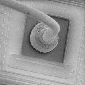
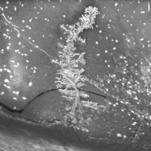
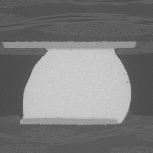
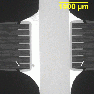
Failure Analysis Examples of Devices, Materials, Cross-Sections and Miscellaneous
At SEM Lab, Inc. our goal is to identify the root cause failure mechanisms. This involves working with our clients to determine the scope of analysis required to achieve this goal. The failure analysis process may include external visual inspection, photography, electrical measurements of the samples, which is often followed by other techniques (optical, SEM, EDS, FTIR, X-ray, and other measurements) to analyze the material and/or the failure. When the analysis is complete, a comprehensive report is provided to the client. Below is a collection of examples of failure analysis divided into sections.
Microscopy and Scanning Electron Microscopy (SEM) images are often necessary to adequately determine a root cause failure mechanism and the resulting images are used to document the analysis. Below are some links to failure analysis examples of samples analyzed at SEM Lab, Inc. They are divided into 4 sections: Devices , Materials, Cross-Sections and Miscellaneous. The devices section includes device failures seen in assemblies, printed-circuit-boards (PCBs), printed-wiring-boards (PWBs), and electronic components such as integrated circuits (ICs), memory chips, transistors, diodes, capacitors, resistors, LEDs, power modules, and many others. Examples of failure analysis of materials includes metals, plastics, ceramics, glasses, and unknown particles. Cross sections are often important to evaluate the internal construction of encapsulated components and assemblies during root cause failure analysis, and several examples are shown in this section. The miscellaneous category is examples of failure analysis that do not fit into the other categories.
On-going current examples of failure analysis can be found on the SEM Lab, Inc. blog.


