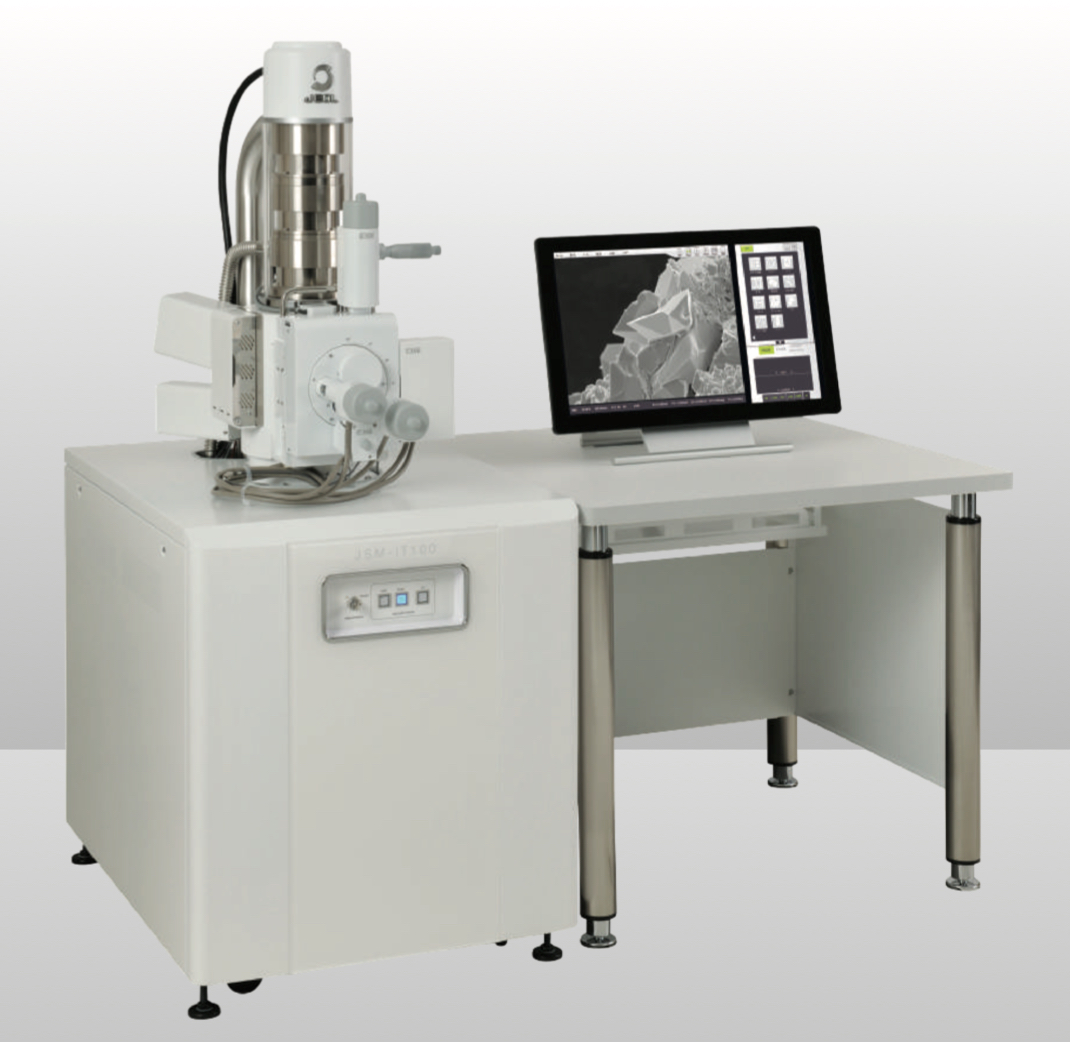
 Jeol JSM-IT-100
High resolution SEM with EDS for elemental analysis and variable (low) pressure control for imaging without evaporated coating.
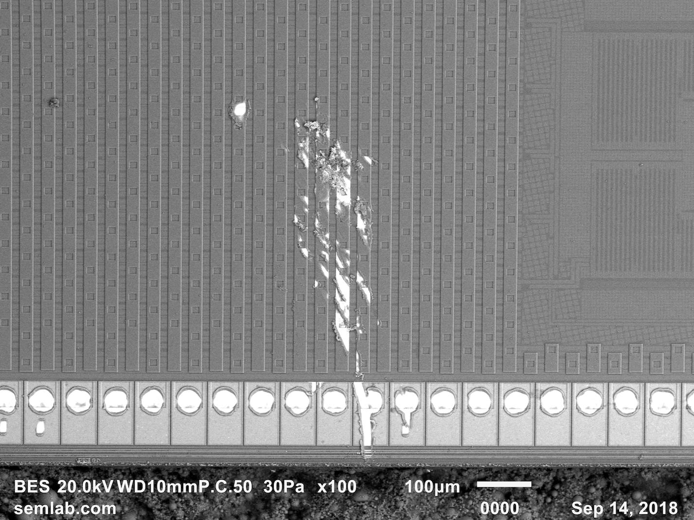
BSE SEM image of a chemically decapsulated integrated circuit showing mechanical damage on the die surface.
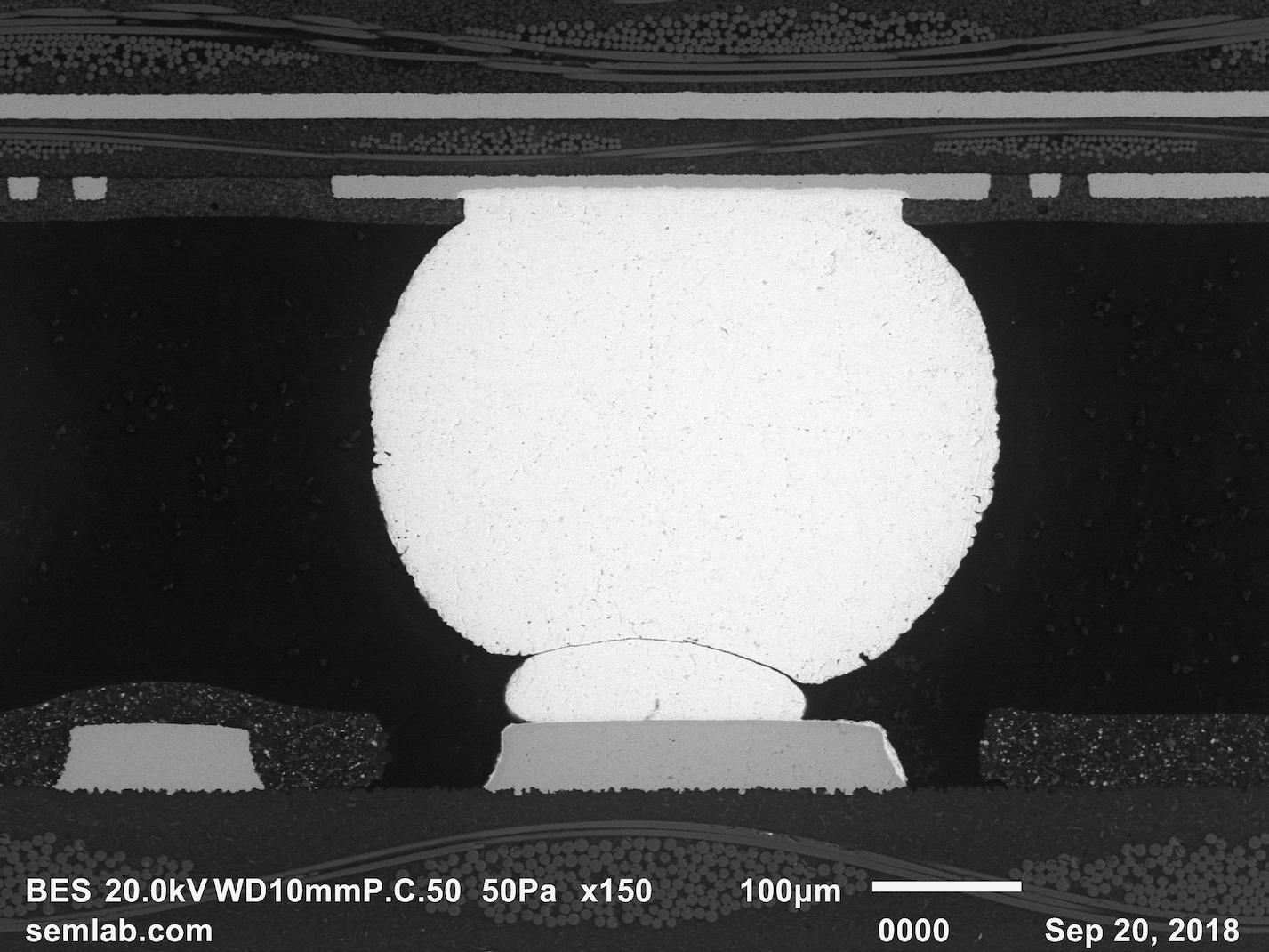 BGA Solder Joint
BSE SEM image of an electrically intermittent solder joint as found in a microsection of the BGA assembly.
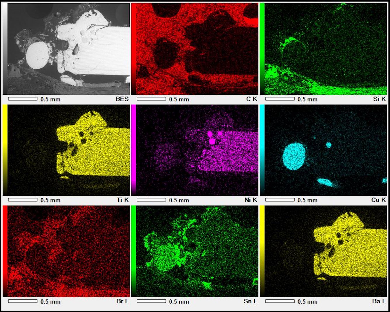 ELEMENTAL MAP
Elemental map of a micro-sectioned multilayer ceramic capacitor (MLCC) that had shorted internally.
Announcing that we acquired a new Jeol JSM-IT-100 SEM capable of the following:
- Higher resolution
- Better elemental mapping
- ZAF quantification with standards
Keep us in mind for your failure analysis and scanning electron microscopy (SEM) needs.
Best Regards,
Ed Hare, PhD
SEM Lab, Inc.
425-335-4400
Join our SEM Lab, Inc. Blog!
Follow our failure analyses….