
Surface trace fractured on rigid-flex assembly.

Location of fracture in microsection.

The stiffness of the PTH solder joint far exceeds that of the trace leading to fracture at the transition.
Check out SEM Lab, Inc. to learn more.
Surface trace fractured on rigid-flex assembly.
Location of fracture in microsection.
The stiffness of the PTH solder joint far exceeds that of the trace leading to fracture at the transition.
Check out SEM Lab, Inc. to learn more.

Optical image of HEXFET® Power MOSFET.
The breakdown site is located near the source wire bond.

This is a higher magnification image of the breakdown site.
The breakdown current in amperes can be roughly estimated by the radius of the “hot spot” or breakdown site [1]. The breakdown current is estimated at ~ 1 amp/1 mil radius.
[1] J. T. May, “Limiting Phenomena in Power Transistors and the Interpretation of EOS Damage”, in Microelectronics Failure Analysis Desk Reference, 3rd Edition, ASM International Press, 1993, pp. 321-328.
Check out SEM Lab, Inc. to learn more.

BSE SEM image of BGA microsection.

The entire interface fractured between the Ni-Sn intermetallic layer and the Ni-P of the ENIG board pad. This is the corner ball where warpage strains are at maximum typically.

Evidence of “hyper-etching” of the Ni-P grain boundaries, which is a symptom of black-pad-syndrome.

This is a recent example of “hyper-etching” of the Ni-P grain boundaries on an ENIG finished PWB that could be described as moderate relative to the previous example. This is the fracture surface of the PWB pad where a BGA was sheared off in what we refer to as “pry & SEM” evaluation. The phosphorus concentration at the fracture surface was determined to be 17.4 wt%, which is elevated compared with the expected 7 – 9 wt% phosphorus for medium phosphorus electroless-nickel. The elevated phosphorus and brittle fracture at the Ni-P/Ni3Sn4 interface are consistent with black pad syndrome, though this appeared to be a marginal case.
Check out SEM Lab, Inc. to learn more.

20 AMPERE, POWER TRANSISTOR, COMPLEMENTARY SILICON, 140 VOLTS, 250 WATTS. It is hard to dump 250 watts through a poor die attachment (the die attach silver-epoxy is not centered on the die).
Check out SEM Lab, Inc. to learn more.

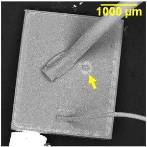
This is a secondary electron SEM image of a blue InGaN LED die after chemical decapsulation.
Check out SEM Lab, Inc. to learn more.

Pure tin plating is problematic especially in applications like flex connectors where mechanical stress is a given.

Here is a tin whisker just off of the crimp connection.

Here is a second tin whisker.
Check out SEM Lab, Inc. to learn more.

BSE SEM image of stock diode sample.

A crack is present in the glass body.
There were fractures in the glass case near the terminations on all of the stock diodes examined. There is significant risk that these fractures would propagate to failure due to expected assembly and use stresses.
Check out SEM Lab, Inc. to learn more.

EDS shows Teflon (or some other fluorine-rich material) contamination on gold plated contact pads on the PWB.
Check out SEM Lab, Inc. to learn more.

Pure tin plating on this flex cable connector contact produced a tin whisker.
Check out SEM Lab, Inc. to learn more.
Electrically conductive residue and corrosion product on the PWB surface under a BGA likely caused reported electrical faults.

BSE SEM image of conductive residues on the board surface after prying-off the BGA.

EDS spectrum suggests the residue is activated solder flux and dissolved tin.
Check out SEM Lab, Inc. to learn more.