Introduction
Our failure analysis laboratory has seen several cases of the same WLED failure mechanism in the past two years, where the lens material is Ce:YAG phosphor in silicone elastomer and the failures appear to be caused by degradation of the lens material. This paper uses three cases to illustrate this failure mechanism and the failure modes associated with it.
The WLED technology for these cases utilize cerium-doped yttrium alumina garnet (Ce:YAG ) phosphor particles suspended in optically clear silicone elastomer. This material appears to be yellow in color because the phosphor particles convert blue light to yellow light. The phosphor-converted WLED is viable because the combination of blue and yellow appears to the eye as white light.
Ref. [1] states that “The unique silicone polymer utilized in pc-LEDs is stable over a wide temperature range and resistant to yellowing after ultraviolet exposure.” If this is the case, then the failures discussed below were likely caused by some sort of abuse, which is likely related to the intensity of white light being generated by the LEDs or the quality of the thermal designs associated with these applications. The cases discussed below involved very bright LEDs and the thermal designs appeared to be quite good.
Case Histories
Case #1: COB WLEDs
Case #1 is related to a chip-on-board (COB) WLED that reportedly failed within approximately half of its expected life due to color shift toward blue light. EDS analysis (Fig. 1A) suggested that the failure mechanism involved carbon loss. FTIR analysis (Fig. 1B) of the silicone coating from the “New” sample suggested that the silicone is polymethylphenylsiloxane. Furthermore, comparison of the FTIR spectra for “New” and “Fail” samples (Fig. 1C) suggested that the degraded silicone coating on the failed LEDs correlates with the disappearance/weakening of Si-Ph absorption peaks, which implies that the phenyl rings in the compound disappear during the degradation process. This mechanism may explain the loss of carbon in the silicone material shown by the EDS data.

Fig. 1A – EDS results for “New”, “Not-Yet-Failed”, and “Failed” WLEDs (atomic percent) where “(n%)” indicates the estimated amount of life consumed for each condition

Fig. 1B – FTIR spectrum of the silicone coating from the “New” sample (top) along with the best match from our spectral library (bottom).

Fig. 1C – FTIR spectra of the failed (top) and control (bottom) samples.
The loss of carbon in the silicone appears to cause shrinkage and fracture in the coating (Fig. 1D). The fractures provide a path for blue light to escape without phosphor conversion, which might explain the color shift toward blue that was reported as the failure mode.

Fig. 1D – SEM micrograph of Ce:YAG-silicone coating. Bright contrast particles are Ce:YAG phosphor. Intermediate gray contrast material is silicone elastomer. Dark contrast features are fractures in the silicone elastomer.
Case #2: Packaged WLED
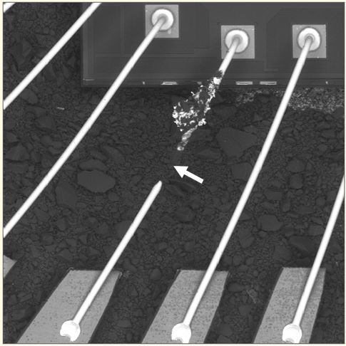
Case #2 is a conventionally packaged WLED that, like case #1, failed within approximately half of its expected life. However, in this case the failure mode was catastrophic with evidence of gross electrical overstress damage. Fig. 2A shows a WLED that remained functional, but showed damage to the Ce:YAG-silicone lens including deep fractures in the silicone that exposed the LED die to the environment. The operating environment in this case was corrosive, and the combination of the fractures in the silicone lens and the corrosive environment led to catastrophic failure as shown in Fig. 2B.

Fig. 2A – WLED that was still functional, but shows damage to the Ce:YAG-silicone lens.

Fig. 2B – WLED that failed catastrophically.
EDS data for the Ce:YAG-silicone lens material for Case #2 showed 50 ± 11 atomic percent carbon (N = 18) compared with 42 ± 6 atomic percent carbon (N=6) for Case #1, which indicates that the silicone material was less degraded on average for Case #2 than for Case #1. This is believed to be because light intensity in the silicone is uniform for Case #1 and varies as a function of location for Case #2. For Case #2, the light intensity is highest directly over the LED die and lower near the periphery of the lens. Since the EDS data was from random locations within the lens for Case #2, the average is skewed to higher atomic percent carbon due to material that was near the periphery of the lens that was not subjected to full light intensity (e.g. Case #3).
Case #3: Packaged WLED2
This case is another packaged LED as shown in Fig. 3A. The failure mode in this case was open circuits caused by failure of either the bond wires or the wire bonds depending on the sample. The lens material is the same type of Ce:YAG-silicone as the previous cases. In this case, EDS data showed 58 ± 10 atomic percent carbon (N = 6) at random locations within the lens material. This was the highest carbon percentage for failed LEDs of the three cases, and for the same reasons discussed in Case #2 it is believed that the average is skewed to higher atomic percent carbon due to nonuniformity of light intensity in the lens material.

Fig. 3A – LED showing two fractures in lens centered on each of two LED dice.
Fig. 3B shows EDS data for the Ce:YAG-silicone lens material of new LEDs and two failed LEDs. The data suggests that there is a loss of carbon for the failed LEDs relative to the new LEDs. Fig. 3C shows a mapping of carbon concentration in the silicone lens material versus location, which demonstrates that the degradation is most severe directly over the LED die where the fractures formed in the lens.

Fig. 3B – EDS data for composition of Ce:YAG-silicone lens of new LEDs and two failed LEDs.

Fig. 3C – Atomic percent carbon versus location relative to the die region of the LED.
Summary
The three cases illustrated above exhibited different failure modes, but they all appear to be caused by the same failure mechanism. This mechanism is characterized by …
- Shrinkage and fracture of the Ce:YAG-silicone lens or coating
- Loss of carbon due to outgassing of VOCs (phenyl groups)
- Unexpected early wearout failure
[1] Pradeep Lall, Hao Zhang, & Lynn Davis, “Failure Mechanisms and Color Stability in Light-Emitting Diodes during Operation in High- Temperature Environments in Presence of Contamination”, 2015 Electronic Components & Technology Conference, 1624 – 1632.