Thin Film Thickness Measurements Using EDS
SEM Lab, Inc. has developed a method for measuring thickness of thin film deposits on various substrates, including multiple layers of different materials, using EDS data. The method is extremely efficient and is therefore a cost effect alternative to conventional and FIB microsection techniques (approximately half the cost).
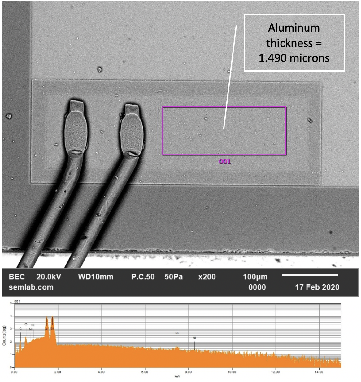
One application for this method is measurement of aluminum deposits on silicon die, particularly wire bond pads. The example below (Fig. A) shows a BSE SEM image and raster scan EDS spectrum of an aluminum bond pad on silicon, and the calculated thickness of the aluminum layer.
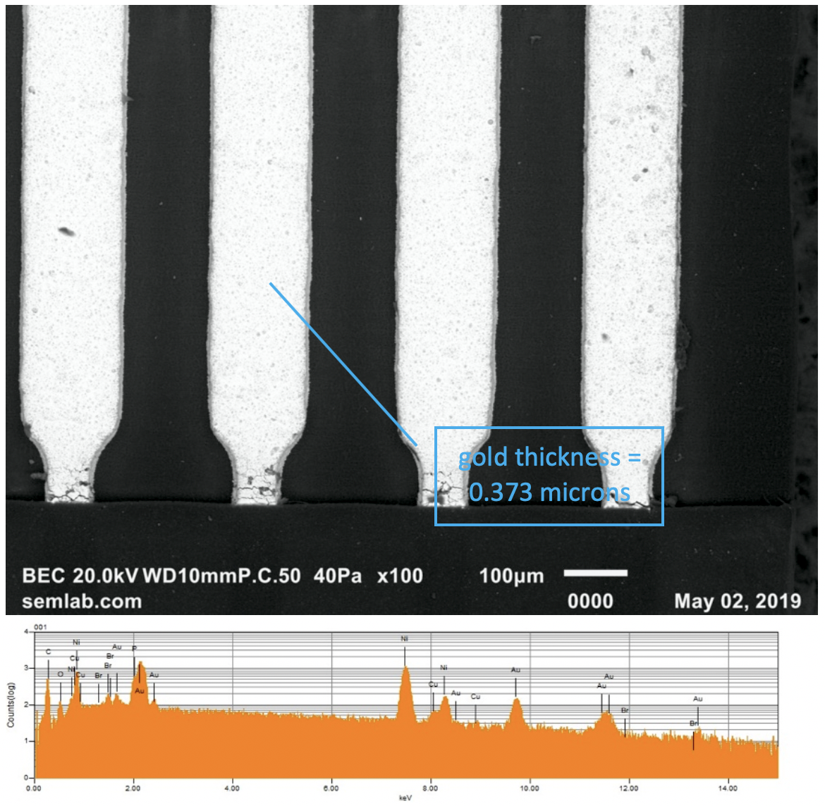
A second example (Fig. B) is gold plating thickness over nickel or nickel-phosphorus alloy. The thickness of the gold layer can be determined for electroless-nickel immersion-gold (ENIG) PWB finishes and thin electro-plated gold (< 15 microns) on boards or component leads.
There are numerous other applications for this measurement method, which has significant advantages over conventional direct measurements on cross-sections including,
- Measurement requires only one EDS spectrum versus multiple direct measurements from cross-sections to achieve a meaningful average
- Non-destructive to the location being examined
- Simultaneous acquisition of image to document surface morphology
- Approximately half the cost of conventional and FIB microsection techniques
In summary, SEM Lab, Inc. can provide thickness measurements of thin film deposits on various substrates, including multiple layers of different materials, using EDS data for approximately half the cost of conventional and FIB microsection techniques. Please contact us to discuss your specific requirements for measurements of thin film deposit thickness.


 August 2002


