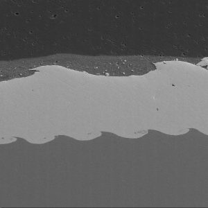
In the previous two decades, black-pad-syndrome was a leading cause of intermittent BGA electrical failure. In 2018, this seems to have been replaced by head-in-pillow defect. Both of these conditions generally require microsection analysis for a conclusive diagnosis as non-destructive techniques mostly fail to identify a problem. Here are some examples of head-in-pillow defect analyzed at SEM Lab, Inc.

Head-in-pillow defect at ball-A3

Head-in-pillow defect at ball-B5

This condition is primarily caused by thermal-mechanical warpage of the BGA during the solder reflow process. Some corrective action recommendations can be found in [1].

[1] SMT Troubleshooting Guide, “BGA Head-on-Pillow”, www.alpha.cooksonelectronics.com, Issued 10/08, p. 17.

An IR LED was submitted for failure analysis. The LED had failed during process validation testing.

These are optical images of the IR LED documenting the results of external examination.

This image shows a microsection just after grinding into the cup. The angle of the gold bond wire near the wire bond appeared to be anomalous.

The open-circuit failure was caused by bond wire fracture that occurred just above the wire bond.

This is a higher magnification image of the fractured bond wire.

The failure was most likely caused by thermal (or possibly mechanical) stress putting tension on the bond wire, and there may have also been some damage to the bond wire as a result of the original wire bonding process during fabrication of the LED.

A Dual Operational Amplifier IC was submitted for failure analysis.

This is an optical image of the device.

This is a BSE SEM image of the device after chemical decapsulation.

This is a higher magnification image of the device die.

This is electrical over-stress damage associated with an output, OUT2.

This is an elemental dot map that shows aluminum exposed through the passivation layer in the damaged areas.

The analysis results suggested that the device failed on OUT2 due to a high voltage transient event on the OUT2 signal.

A client provided several PCBAs for failure analysis of out-of-tolerance MELF resistors.

This is an optical image of a typical failed resistor showing localized delamination of the protective coating from the Tantalum thick film resistor material and Sn-Pb particles trapped at the interface.

This is a high magnification optical image of a Sn-Pb particle as-viewed through the outer coating that bridged the laser cut causing a short.

This elemental spectrum shows that the short is a Sn-Pb particle (sample particle as in previous image).

Sn-Pb particles were found in microsections sitting on top of the Tantalum thick film resistor material under ~ 40 microns of outer coating.

The root cause of the failures was tramp metal (Sn-Pb) contamination under the coating suggesting inattention to cleanliness in the manufacturing environment. I am left wondering why the manufacturing operation didn’t use AOI techniques (or human inspection of samples) to prevent this from getting out of the factory. The loss of reputation seems to be a cost greater than the investment in AOI.

This is an optical image (bottom-view) of a surface mount transformer.

This is a BSE SEM image of a microsection through the transformer.


If the image contrast is appropriate, image analysis software can be used to count and measure feature location and geometry.

In this case, the count and diameters of the conductors is summarized.


This is an optical image (top view) of an LED that failed open circuited.

The next image is a side view of the microsectioned LED. This fracture shows striations (red arrow) propagating away from the bond wire. There is also a discontinuity in the bond wire (white arrow) that appears to be the break that explains the open circuit condition.

How can this damage be explained? The CTE of cast epoxy (the body/lens) is ~55 ppm/C and the CTE of gold (the bond wire) is ~14 ppm/C. So the epoxy thermally expands ~4X more than the gold for a given temperature excursion. It seems likely that the break in the gold bond wire occurred due to an increase in temperature, which would put the gold wire in tension. On the other hand, it seems likely that the fracture in the lens material occurred due to cold temperatures (or alternatively due to pulse heating of the bond wire) where the epoxy just of the gold/epoxy interface would be in tension. In any case, our experience shows that LEDs tend to fail if forward current and ambient temperatures approach the maximum operating limits in the LED specification. Since lighting applications are often pushing for maximum lumens (maximum forward current and power dissipation), many failures could be avoided by applying derating principles at the design stage.

Chip components such as MLCCs, high value (~ 1Mohm) chip resistors, and transorbs that fail due to excessive electrical leakage are often not component failures at all, but rather are SMT design/process induced failures.  For example, the chip component illustrated below exceeded the component level specification of < 1 uA leakage.

In this case, the excessive leakage condition in-circuit was attributed to tin residue on the board surface under the chip component.  The suspect component was mechanically removed and the board surface was examined in a SEM.  The BSE SEM image (top) showed a residue on the board surface between the two terminals of higher average atomic number than the solder mask.  An elemental map for tin (bottom) showed that the tin residue was essentially continuous across the isolation space.

Three possible factors that can contribute to these residues are (1) design – the capillary gap, terminal spacing, and applied voltage are factors, (2) process – the cleaning process and/or solder flux selection may be inadequate, or (3) electromigration – the bias voltage, ionic residues, and humidity cause electromigration of tin across the isolation gap with time. The root cause is often a combination of these factors. 

A microcontroller IC was failing at apparently random I/O pins.

This is an optical image of the chemically decapsulated device.


This is a BSE SEM image of the decapsulated device.


This image shows a displaced ball bond with an elemental spectrum of the bottom of the crater.


This is a higher magnification image of the bond crater.

Bond cratering can occur at apparently random bond pads likely due to variation & non-perfect planarity of the die attachment.

A PCBA was provided to SEM Lab, Inc. for evaluation of some QFN solder joints.  This is a BSE SEM image of a microsection of the QFN.

The solder joint geometry appeared to be acceptable in this section. There was a uniform layer of Cu-Sn intermetallic at both the solder/pad and lead-frame/solder interfaces suggesting that the reflow profile was acceptable.  The interfacial intermetallic layers also suggest that there was no solderability problem associated with the QFN or PWB pads.

This is a 2nd section plane that included the thermal pad under the QFN.  The level of solder fill in the PTH-vias under the thermal pad was variable.

The “toe” of the solder joints shows an excess-solder condition possibly because of the balance of forces caused by solder surface tension between the signal solder joints and the thermal pad, which determines the solder joint height.

One possible solution for mitigating these issues is to fill the PTH-vias as illustrated in the image below.