A client provided a failed CMOS Flip-Flop IC to SEM Lab, Inc. for failure analysis. An output signal reportedly failed when the circuit was connected to an electronic counter.

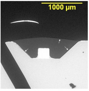
This is a BSE SEM image of the device after grinding through the alumina ceramic top of the CerDip package into the die cavity. The bond wires on the device were found to be intact.

SEM examination of the die area associated with the output signal revealed that the metal run between the wire bond pad and the first contact on the die was fused open.

This is a higher magnification image of the metal run between the wire bond pad and the contact that fused open.

The dimensions of the fused section of metallization and the bond wire were estimated and input into a model for calculation of the electrical overstress (EOS) event pulse width. The pulse width was estimated as in the range of 1-100 microseconds, which is consistent with a high voltage transient EOS event.

This image shows the same output area on a known good device for comparison.
The analysis results suggested that the electronic counter associated with the failure should be investigated for proper grounding.


