A client requested microsection analysis of a drop tested assembly. Examples of the types of damage found are shown below.


Check out SEM Lab, Inc. to learn more.
A client requested microsection analysis of a drop tested assembly. Examples of the types of damage found are shown below.
Check out SEM Lab, Inc. to learn more.
This is a fairly typical example of wear out failure of an aluminum electrolytic capacitor.

This is an optical image of the capacitor that captures the part date code.

This is an image of the top of the device showing the vent, which ruptured and leaked a small amount of electrolyte.

This is an image of the capacitor after dissecting the can. The capacitor roll was charred indicating that the core reached excessive temperature.

This is a plot of capacitance versus age for “passing” capacitors from the same population of capacitors. The trend line is an inverse exponential function indicative of the wear out process.
The analysis results suggest that the capacitor failure was caused by the normal wear out processes that are characteristic of aluminum electrolytic capacitors, i.e. capacitance decreases and electrolyte volume decreases (i.e. capacitor dries out) as the capacitors age and approach end-of-life.
Check out SEM Lab, Inc. to learn more.

A client suspected a tin whisker had grown between two IC leads.

It turns out this was a glass fiber embedded in the solder joint.

EDS analysis proves it is a SiO2-Al2O3-CaO glass fiber.
Check out SEM Lab, Inc. to learn more.
This is a somewhat classic case of solder joint fatigue failure, but with the added factor of gold embrittlement. The solder alloy is SN63, the package is a J-lead PMIC, and it is soldered to an alumina ceramic substrate.

The elemental spectrum of the bulk solder joint suggested it contained ~ 3 wt% of gold, which is considered a threshold for gold embrittlement.

The thermal fatigue fracture showed classic characteristics such as grain boundary separation and propagation through the bulk solder joint.

The AuSn4 intermetallic compound is clearly visible in the solder joint microstructure at about 12% by area in the section. This harder phase in the Sn-Pb matrix likely accelerated the thermal fatigue failure.
The analysis results suggest that the thermal fatigue damage was likely due to the combination of (1) CTE mismatch between the J-lead package and the alumina substrate and (2) Au-Sn IMC in the solder joint microstructure at the threshold for gold embrittlement.
Check out SEM Lab, Inc. to learn more.
LEDs tend to develop high levels of thermal expansion mismatch stress internally due to gross CTE mismatch between the lens polymer, the die, the lead-frame/cup, and the bond wires. In the case shown below, a silicone polymer was used to fill the cup perhaps to provide a stress buffer, but it did not appear to be effective.

This view (photo above) is looking down through the lens at the die area. The damage shown is at the interface between the body material and the silicone polymer that fills the cup and encapsulates the device die.

There was no evidence of damage at the wedge bond.

This view (above) is a look through the bottom (lead) side of the device. There appeared to be some crazing at the rim of the cup.

This image (above) was obtained at an intermediate stage in the microsectioning process. There is a fairly significant kink in the bond wire above the ball bond.

The silicone encapsulant adhesively failed at the cup/silicone interface and the silicone/lens polymer interface.

The image above shows a segment of silver plating that has separated from the underplating on the cup.
Above is an optical image showing the location of the open at the kink, which is the high stress region of the gold bond wire.
Conclusion – The analysis results suggest that the LED failed due to an open bond wire just above the ball bond on the device die. The damage was likely caused by a thermal overstress event where the thermal expansion rate of the silicone die encapsulant and the peak temperature are the primary drivers. The kink in the bond wire and the adhesion strength between the silicone die encapsulant and the cup were also a likely contributing factors.
Check out SEM Lab, Inc. to learn more.
Residues on PCBAs are unfortunately common place. SEM/EDS analysis helps to determine the nature of the residue.

The image above shows residue on the surface of the PCBA, but it is not clear what is the nature of the residue.

EDS analysis shows that the residue is likely tin bromide, suggesting corrosive bromide flux activator was left behind after assembly.

This is a BSE SEM image of some of the residue, which shows dendritic growth. The dendrites suggest that electrochemical migration (ECM) was a factor meaning ionic contamination, electric field, and moisture were likely at play. If the dendrites migrate between normally isolated signals (e.g. PWR & GND) then the circuit fails.
Check out SEM Lab, Inc. to learn more.
A client provided two sensor assemblies for failure analysis of capacitor C4 on the internal PCBA.

This is an optical micrograph of the capacitor as mounted on the PCBA.

This is an optical image of an intermediate grinding stage during microsection preparation. A bending fracture was noted under one of the terminations.

This is a BSE SEM image of the capacitor microsection.

The fracture appeared to be due to flexure of the PCBA.
Check out SEM Lab, Inc. to learn more.
Ionic contamination, moisture, and electrical bias can combine to create electro-chemical migration (ECM) shorts under an IC device as shown in this example.

This is an optical image showing residue on the bottom surface of the FPGA package.

This is a BSE SEM image of the same corner location. The residue bridges several signals at this corner.

An EDS spectrum of the residue suggest that it contains chlorine and bromine. Part of the bromine signal likely originates from the brominated epoxy molding compound. The chlorine & perhaps some of the bromine is most likely residual solder flux activator.
The analysis results suggest that the most likely cause of failure was external corrosion and ECM due to halide contamination. The corrosion and ECM was likely exacerbated by elevated temperature and humidity conditions.
Check out SEM Lab, Inc. to learn more.
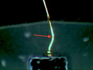
A client provided a flex cable sample to SEM Lab, Inc. for SEM/EDS analysis of the crimp contact plating.

EDS of the contact plating revealed that the plating was pure tin, which explains in part the many tin whiskers associated with the crimped region of the flex cable.

The longest whisker in this image is very close to shorting two adjacent signals.
Check out SEM Lab, Inc. to learn more.
An LED lamp assembly reportedly “flickered”, meaning there was likely an intermittent high resistance in the LED circuit.

Here are summaries of the destructive physical analysis of three suspect LEDs.


The analysis results for all three samples were similar. Thermal-mechanical damage was found including (1) thermal decomposition of the lens material mid-span on the anode bond wire on Sample A & Sample C, (2) adhesive failure (separation) between the phosphor-filled-die-encapsulant and the cup on all samples, and (3) fracture of the phosphor-filled-die-encapsulant that intersected the cathode ball bond of Sample B. All of these observations are consistent with the thermal-mechanical effects of electrical overstress.
The client reported that the LEDs were being operated at 150% of the maximum forward current, which likely was the primary factor causing premature failure.
Check out SEM Lab, Inc. to learn more.