Corrosion due to residual solder flux and cleaning process chemistries left on PCBAs can be a real problem for reliability. The corrosion can cause both open circuits as it eats through metal runs and short circuits due to electro-chemical migration.

Pixel_Size=1.25003E+1 µm Mag=13.890 × Display_Mag=158 Zoom=6.33000 Stage_X=-11.299 mm Stage_Y=-8.815 mm Stage_Z=0.000 mm Stage_R=0.00° Stage_T=0.00° Stage_B=0.00° Spot_Size=29.3% Accelerating_Voltage=15.0 kV Working_Distance=21.9 mm Operator=SEM Lab Instrument=PSEM II Analysis_Date=1/6/2011 Analysis_Time=02:10:10 PM Sample_Number= Client_Number= Client_Name= Project_Number= Caption= RasterBox=[119,233,375,284] Live_Time=78.00 Acquisition_Time=91.00 Dead_Percent=11.0% Detector_Tilt=35° Peak_Label=Cr@5.414 Peak_Label=Cr@5.946 Peak_Label=Ni@7.477 Peak_Label=Ni@0.851 Peak_Label=Fe@6.403 Peak_Label=Fe@7.057 Peak_Label=Fe@0.705 Peak_Label=Sn@3.904 Peak_Label=Sn@3.443 Peak_Label=Sn@3.662 Peak_Label=Br@1.481 Peak_Label=Pb@2.345 Peak_Label=Cl@2.622 Peak_Label=Si@1.741 Peak_Label=C@0.277 Peak_Label=O@0.525

This (above) is the elemental spectrum of the end of a through-hole connector solder joint. The chlorine in the spectrum is likely due to chloride activator from the solder flux.

Pixel_Size=1.24996E+1 µm Mag=13.891 × Display_Mag=160 Zoom=6.41000 Stage_X=-11.169 mm Stage_Y=-8.048 mm Stage_Z=0.000 mm Stage_R=0.00° Stage_T=0.00° Stage_B=0.00° Spot_Size=29.3% Accelerating_Voltage=15.0 kV Working_Distance=21.5 mm Operator=SEM Lab Instrument=PSEM II Analysis_Date=1/6/2011 Analysis_Time=02:07:24 PM Comment= RasterBox=[250,245,273,286] Live_Time=65.00 Acquisition_Time=78.00 Dead_Percent=14.0% Detector_Tilt=35° Peak_Label=Sn@3.904 Peak_Label=Sn@3.443 Peak_Label=Sn@3.662 Peak_Label=Br@1.481 Peak_Label=Ba@5.156 Peak_Label=Ba@4.827 Peak_Label=Ba@4.465 Peak_Label=Pb@2.345 Peak_Label=Cl@2.622 Peak_Label=Si@1.741 Peak_Label=C@0.277 Peak_Label=O@0.525

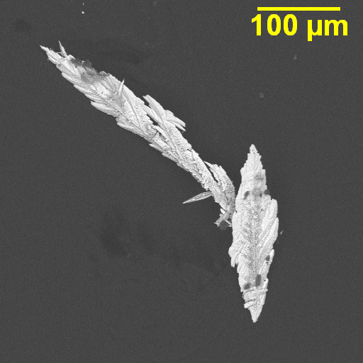
This (above) is the elemental spectrum of some corrosion product associated with the through-hole connector solder joint, which appear to be Pb and/or PbO crystals growing out of the surface of the solder joint.

pcba-corrosion-3

These are the Pb and/or PbO crystals growing out of the surface of the solder joint.

Check out SEM Lab, Inc.  to learn more.

Electrical continuity tests suggested that the gate was shorted to the drain and the source was intact. SEM analysis revealed a suspected damage site at the end of a gate finger (see below).

shorted-fet-1

An elemental dot map at the breakdown site showed some slight disturbance of the aluminum metallization at the site.

shorted-fet-2

Voltage contrast imaging confirmed that the suspect damage site was indeed the location of the short.

shorted-fet-3

These results suggested that the device failed due to a voltage transient on the gate signal. The small dimensions of the damage site suggest that the transient was very fast (rough estimate 1E-9 to 1E-6 seconds). The damage could potentially be related to an ESD event. It could also potentially be caused by accumulated damage at the tips of the gate contacts due to excessive turn-on or turn-off dV/dt.

Check out SEM Lab, Inc.  to learn more.

Here is another example of electro-chemical migration that resulted in shorted signals on a printed circuit board assembly.

dendritic-growth-1

These ECM residues can often be hard to see under an optical microscope because there are optically transparent metal oxides present with very small metallic dendrites.

dendritic-growth-2

Backscattered electron SEM images show contrast related to atomic number, so for example lead appears very bright (Pb z=82) and carbon appears dark (C z=6). The dendritic structure is a clue that this was ECM related.

dendritic-growth-3

The elemental map below shows that the dendrites are mostly lead but there is also some tin. Both lead and tin are likely to be involved for Sn-Pb solder joint assemblies.

dendritic-growth-4

Check out SEM Lab, Inc.  to learn more.

ECM (electro-chemical migration) can occur when moisture, voltage bias, and ionic contamination come together, such as was the case for the PWB battery contacts shown in the BSE SEM image below.

battery-contacts-1

Elemental analysis suggested that the ECM residues were primarily copper, but also zinc (from brass?) and nickel (from ENIG finish or nickel under-plate on the connector contact?).

battery-contacts-2

The feature that identifies this as ECM versus plain chemical corrosion is the dendritic structure of the residue as shown in the next image.

battery-contacts-3

Historical data from this laboratory shows that the most significant factor is often moisture, followed by voltage (or local electric field), and finally ionic contamination. The lesson seems to be “keep it dry”.

Check out SEM Lab, Inc.  to learn more.

Design rules suggest that MLCCs should be placed away from board edges and panel break out zones for reasons illustrated in this example.

The MLCC was placed far too close to the breakout feature during the design phase for this product.

This is a higher magnification image of the flexure fracture that caused the MLCC to short circuit some time after the board was placed into service.

Check out SEM Lab, Inc.  to learn more.

This example is a SMT connector where the solder joint appeared suspect.

creep rupture 1

Below is a BSE SEM image of a microsection through the suspect solder joint and its neighbors. Note the coplanarity issues for these connector leads.

creep rupture 2

This appeared to be a creep rupture failure of the solder joint where the lead that failed was under stress that caused creep (time dependent plastic deformation) of the solder joint. The vertical displacement of the lead after the solder joint fractured is the key feature that suggests this was a creep rupture failure.

creep rupture 3

Check out SEM Lab, Inc.  to learn more.

Tombstoning is a well known issue for SMT soldering and is usually caught at post solder visual inspection. However, at times the effect is a subtle lifting at one end of the component as was the case in this example of an SMD inductor. The failure was a high resistance in the associated signal net that wasn’t detected until final assembly and testing of the product.

Tombstone1

This is a BSE SEM image of a microsection of the device as soldered on the PCBA.

Tombstone2

The high resistance was caused by a failure of the original solder reflow process to wet the termination, which caused “tomb stoning” of the inductor.

Check out SEM Lab, Inc.  to learn more.

Silver is a common material used to connect resistor terminals to the resistive element within the resistor. This example shows some unknown crystals growing out of the termination area.

These crystals are shown in the BSE SEM image below.

EDS analysis showed that these are silver sulfide crystals.

These crystals most likely formed as a result of gaseous sulfur corrosion of the silver thick film conductor near the termination of the resistors. Corrosion such as the type seen here is typically due to atmospheric sources of sulfur such as diesel fuel fumes or out-gassing from cardboard.

Check out SEM Lab, Inc.  to learn more.

Sometimes IC bond pad corrosion is caused by residual process chemistry from the die fabrication or packaging process as was the case in this example.

Screen Shot 2016-08-18 at 9.37.10 AM

The decapsulated IC showed corroded aluminum bond pads.

Screen Shot 2016-08-18 at 9.38.15 AM

EDS results showed a clear chlorine peak associated with the corrosion.

The corrosion caused signals to open circuit resulting in device failure.

Check out SEM Lab, Inc.  to learn more.

Crystal frequency shift

This is a BSE SEM image of a quartz crystal that reportedly shifted in frequency. The problem was apparently caused by tin-lead solder on the spring mounts that wicked out onto the silver contact metallization on the crystals, which would be expected to change the mechanical response and therefore the frequency of the crystal.

Check out SEM Lab, Inc.  to learn more.