Fine pitch SMT device with wetting problem associated with the device leads.

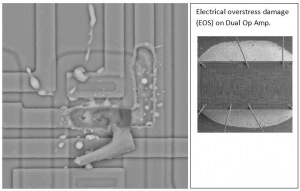
Electrical overstress (EOS) damage on metallization run on Op-Amp IC.

Laminate Damage.

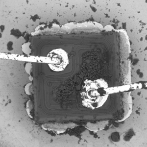
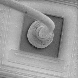
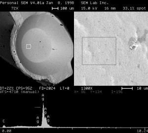
IC Failure Analysis: Gold wire bond on aluminum die pad on decapsulated plastic molded IC.

Exposed copper at plated through holes due to a processing problem.

Hot air solder leveled PWB shows exposed Cu-Sn intermetallic compound. This caused severe wetting problems during assembly.

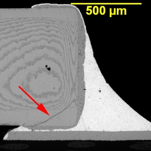
This is a flex crack in MLCC caused by breakout of PCBA from panel. The PCBA layout during the design phase is critical in preventing this type of failure.

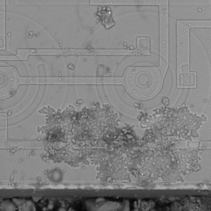
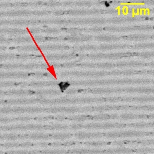
Particle residue found on contact region in dissected relay device.

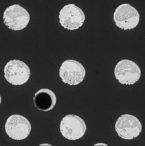
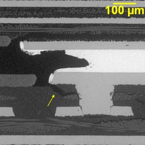
PWB Failure Analysis. PWB inner layer separation of internal land from PTH plating.

Crystal frequency shift.

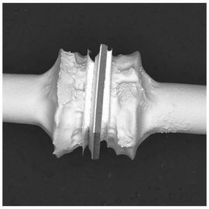
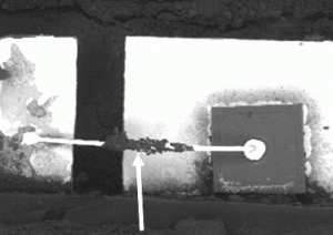
EOS failure resulted in fused bond wire.

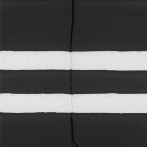
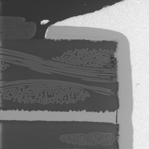
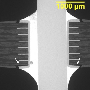
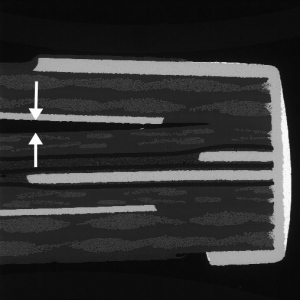
Failure analysis of a PCB showing a parallel section of an inner layer. A crack propagated through these copper traces.

Failed Diode.

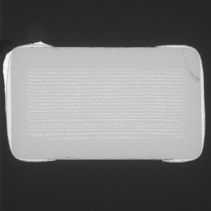
Flexure crack in an MLCC.

Transistor failure caused by electrical overstress damage across most of the emitter region of the die.

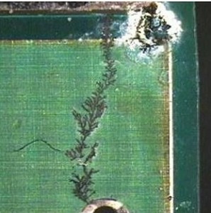
Electromigration short on PCBA

PTH Pad Lift

LED Die Fracture

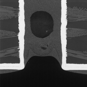
This is a dielectric void in a base metal electrode (BME) multilayer ceramic capacitor (MLCC).

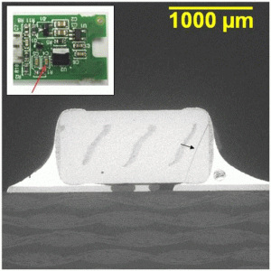
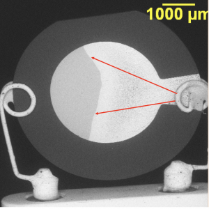
LED microsection where the open circuit failure was caused by the die and lens material separating from the bottom of the cup and rupturing the die attachment.

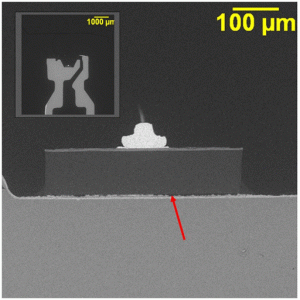
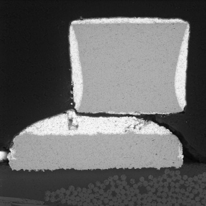
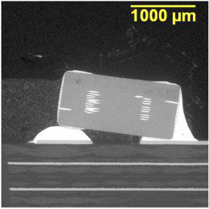
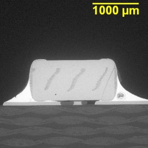
BSE SEM image of a microsection of the device as soldered on the PCBA.

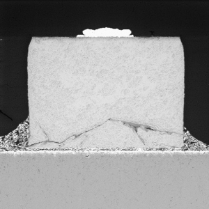
MLCC Bending Fracture

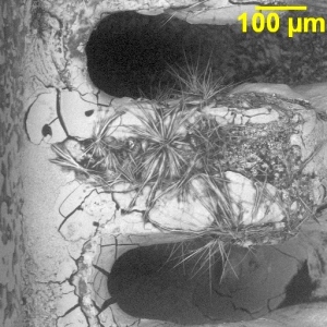
This crystal growth is the result of electro-chemical-migration (ECM) of the solder finish on the IC leads.

Diode short.

Internal PWB Short

Corroded wire bond on a decapsulated IC.

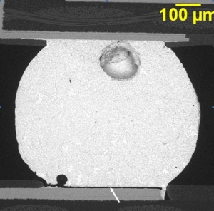
Brittle interfacial fracture of a BGA solder joint.

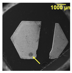
Decapsulated diode

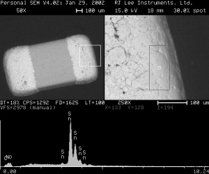
Determination of termination composition on Multi-Layer Chip Capacitor (MLCC).

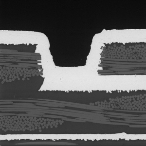
HDI micro-via quality evaluation.

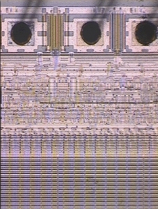
Optical image of a decapsulated EEPROM

Capacitor failure caused by a crack running through several opposing capacitor plates.

Delamination of PWB due to improper oxide treatment prior to lamination.

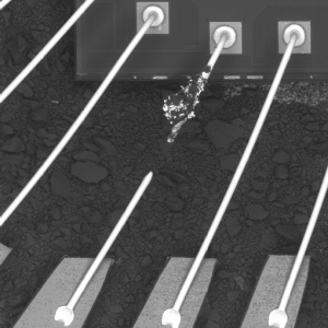
This is a chemically decapsulated SMD diode that failed due to excessive current electrical overstress (EOS). The bond wire fuses open near the center of the span because it is heat-sunk at both ends.

Light Emitting Diode (LED) die bond adhesive failure.

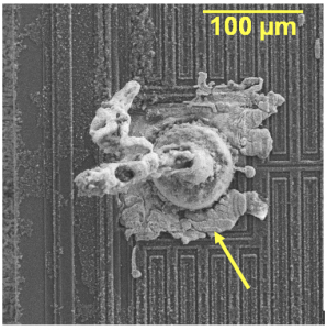
Electrical overstress damage
