LEDs tend to develop high levels of thermal expansion mismatch stress internally due to gross CTE mismatch between the lens polymer, the die, the lead-frame/cup, and the bond wires. In the case shown below, a silicone polymer was used to fill the cup perhaps to provide a stress buffer, but it did not appear to be effective.
This view (photo above) is looking down through the lens at the die area. The damage shown is at the interface between the body material and the silicone polymer that fills the cup and encapsulates the device die.
There was no evidence of damage at the wedge bond.
This view (above) is a look through the bottom (lead) side of the device. There appeared to be some crazing at the rim of the cup.
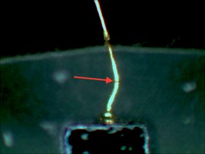
This image (above) was obtained at an intermediate stage in the microsectioning process. There is a fairly significant kink in the bond wire above the ball bond.
The silicone encapsulant adhesively failed at the cup/silicone interface and the silicone/lens polymer interface.
The image above shows a segment of silver plating that has separated from the underplating on the cup.

Above is an optical image showing the location of the open at the kink, which is the high stress region of the gold bond wire.
Conclusion – The analysis results suggest that the LED failed due to an open bond wire just above the ball bond on the device die. The damage was likely caused by a thermal overstress event where the thermal expansion rate of the silicone die encapsulant and the peak temperature are the primary drivers. The kink in the bond wire and the adhesion strength between the silicone die encapsulant and the cup were also a likely contributing factors.
Check out SEM Lab, Inc. to learn more.


