SEM Lab, Inc. Document Collection
This page is a collection of documents and presentations that we have created based on failure mechanisms we have seen in the last 25 years. Please feel free to download the pdf files. Comments are appreciated ( info@semlab.com ).
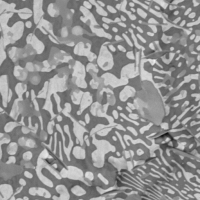 Intermetallics in Solder Joints
 The intermetallic compounds that have been most important in our work performing microstructural evaluations on solder joints are described in this paper.
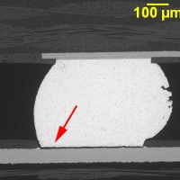 Failure Analysis of BGAs
 This document describes several BGA failure modes and analysis approaches that can be performed with a limited number of analytical tools (e.g. DMM, microsectioning, and SEM/EDS).
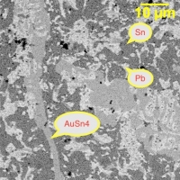 Gold Embrittlement of Solder Joints
 A detailed account of how material and process parameters can lead to gold embrittlement of solder joints in electronic assemblies.
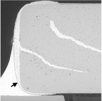 Diffusion Barrier Plating in Electronics
 This paper is a series of examples illustrating the use of diffusion barriers in electronics manufacturing.
 Images of Failures in Microelectronic Packaging
 A collection of images showing failures seen at SEM Lab, Inc. Originally given as an IMAPS presentation.
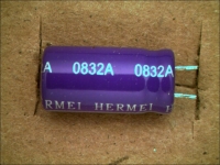 Failure Analysis of Aluminum Electrolytic Capacitors
 A guide to failure mechanisms and failure analysis techniques in aluminum electrolytic capacitors made available on Google Books.
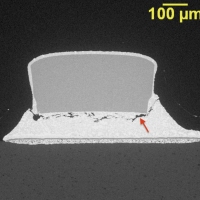 Solder Joint Analysis
 SEM Lab, Inc. has extensive expertise in evaluation and failure analysis of solder joints. This presentation highlights some of these capabilities.
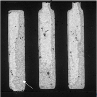 HASL Finish on PWBs
 This presentation discusses how poor HASL quality on PWBs can affect PCBAs. Several examples of poor HASL quality are illustrates with SEM/EDS data. Recommendations are made for mitigation of this recurring quality issue.
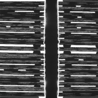 PWB Failure Analysis
 This presentation documents some of the most common PWB failure causes seen at SEM Lab, Inc.
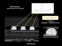 BGA Assembly Verification
 SEM Lab, Inc. provides a comprehensive approach to BGA assembly validation using microsection and SEM analysis. The results can be used to optimize assembly processes early in the product development cycle and help to prevent failure during production. This paper describes this process.
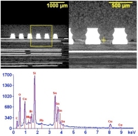 Solder Flux Residue - Part 1
 Solder flux residue left on printed circuit board assemblies often results in corrosion, electro-chemical migration, electrical leakage, and short circuit faults. SEM/EDS analysis of these residues has shown us that various flux chemistries and levels of corrosion can lead to a variety of elemental signatures. This paper investigates what conclusions can be drawn from the EDS data for solder flux residue.
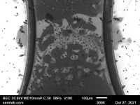 Solder Flux Residue - Part 2
 In Part 1, we mentioned that some of the constituents (e.g. Si, Ba, S) found in the EDS spectra of solder flux residue on a PCBA surface are likely due to the solder mask beneath the residue as the e-beam can penetrate through thin residue layers. Here we examine how to analyze EDS data to remove the contribution of the solder mask.

