Solder Voids
Interfacial Voiding At Nickel Interface
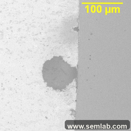
An interfacial-microstructure example where the voiding is concentrated at the solder to nickel-plating boundary rather than appearing as random bulk porosity.
Interpretation
Why this image matters
The voiding is concentrated at the interface itself, which changes the engineering question from simple void count to bonding quality and process adequacy.
The report concluded that the soldering time-temperature profile was not yet optimized and specifically compared sample conditions in terms of voiding and interfacial microstructure.
It is a good image when discussing solder-profile effects instead of treating all voids as the same type of issue.
solder-voids
interfacial-voids
nickel-interface
interfacial-microstructure
Use this when
Best comparison value
- Reference: interfacial voiding versus random bulk porosity
- Discussing solder-process profile adequacy
- Comparing interfacial microstructure across sample conditions
Related content