Electrical overstress
EOS examples
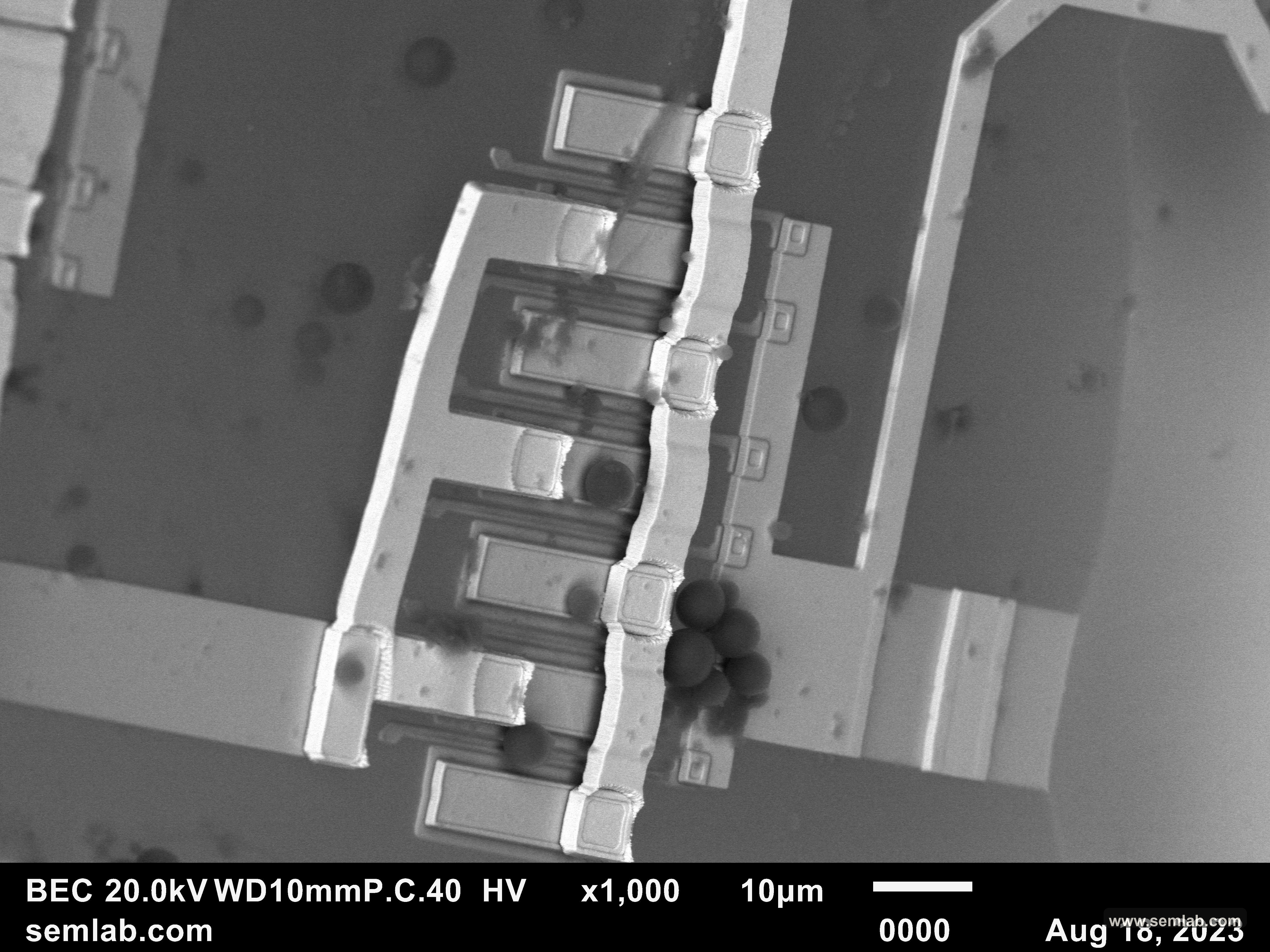
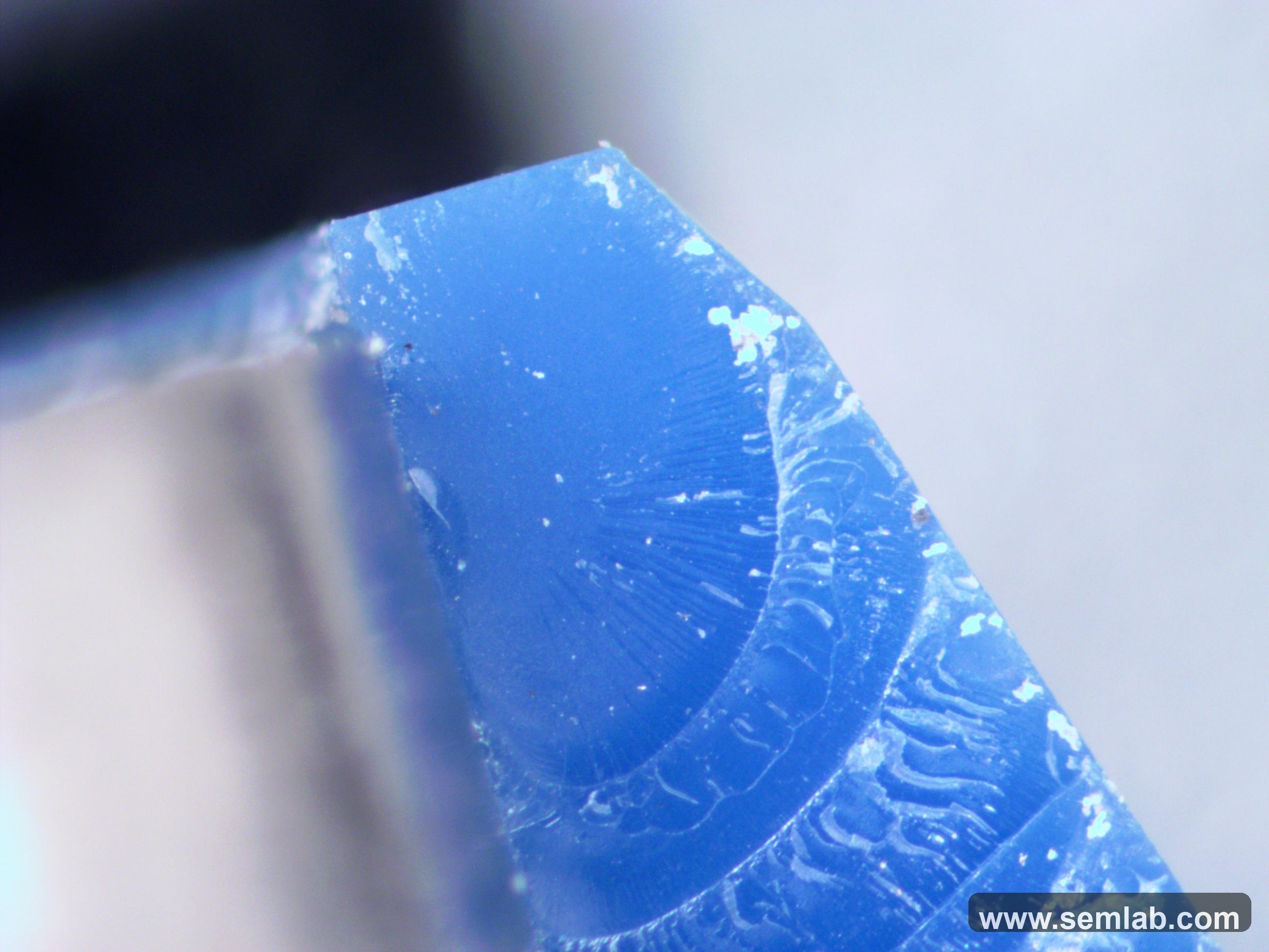
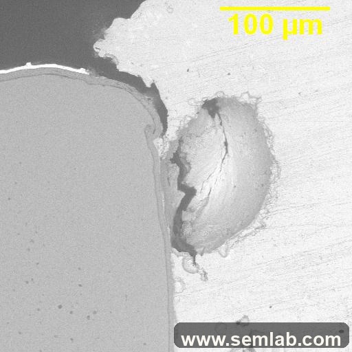
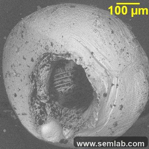
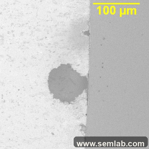
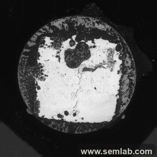
- IC die-level EOS in an output metallization region
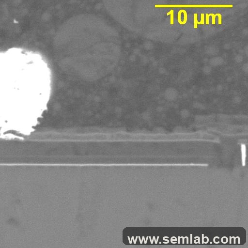
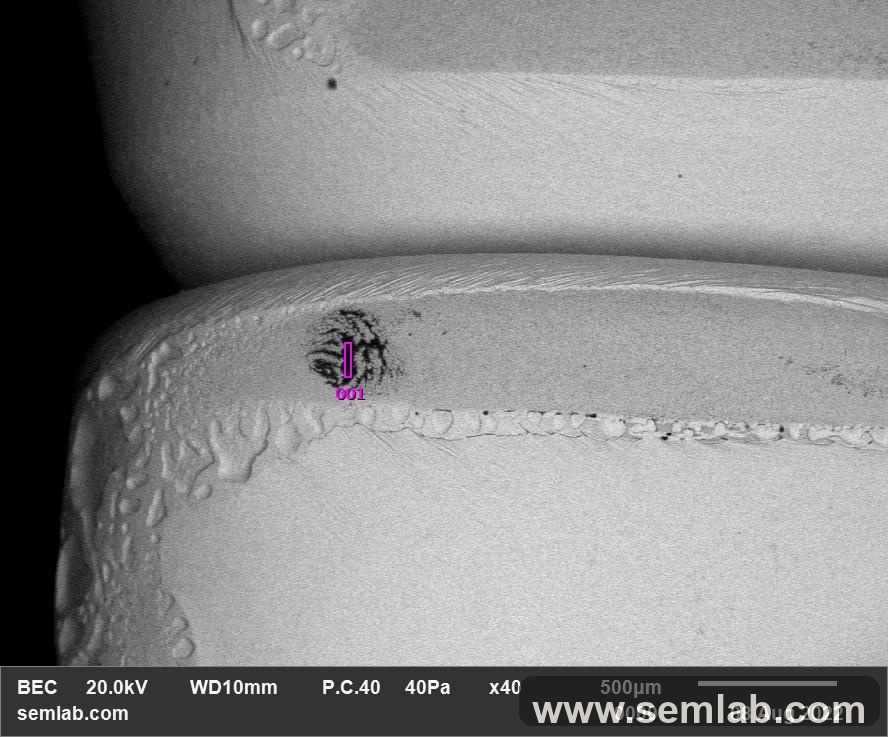
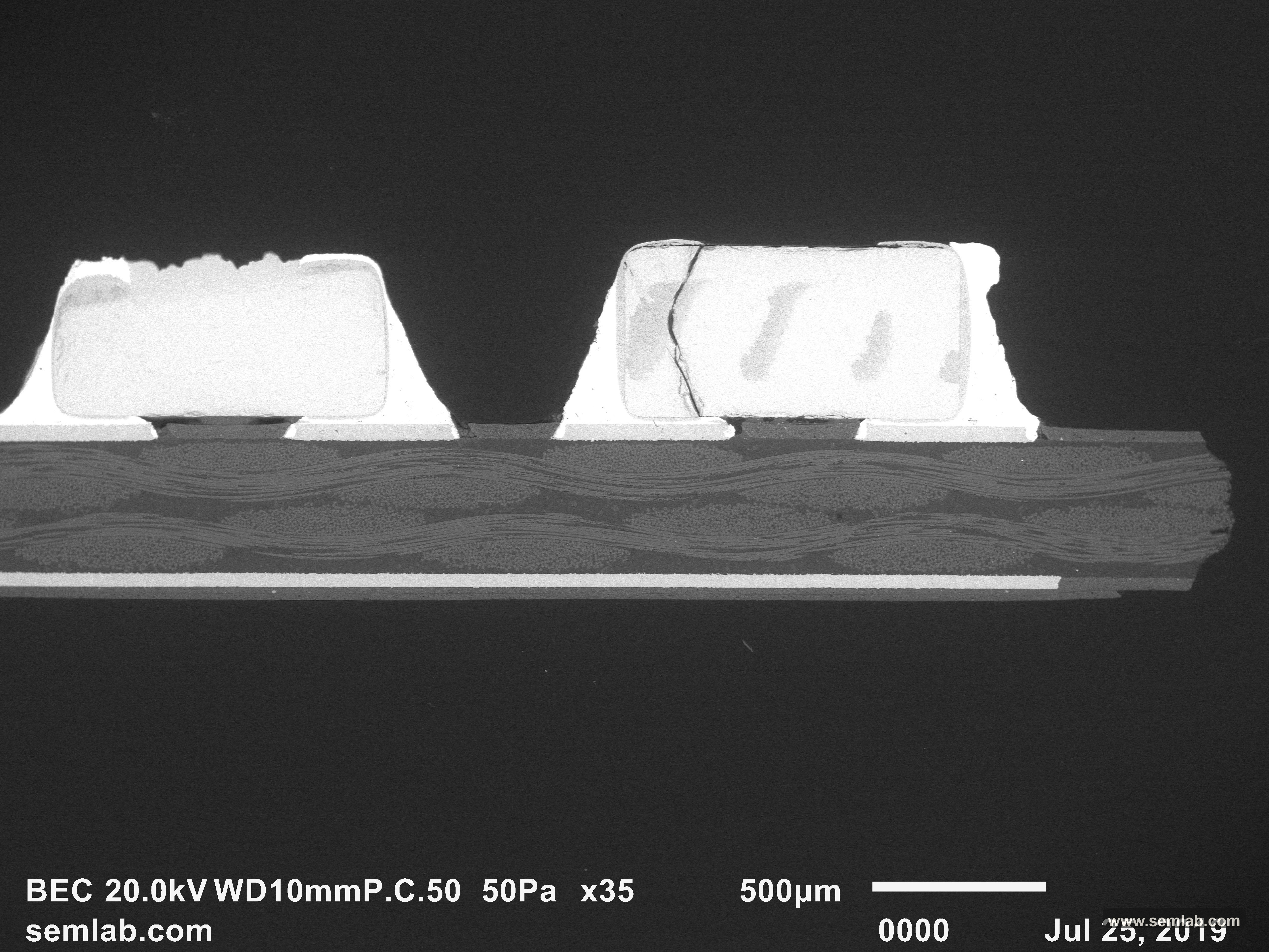
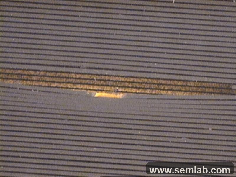
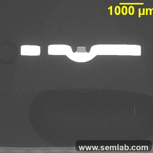
- Fused-open bond wire after current overstress
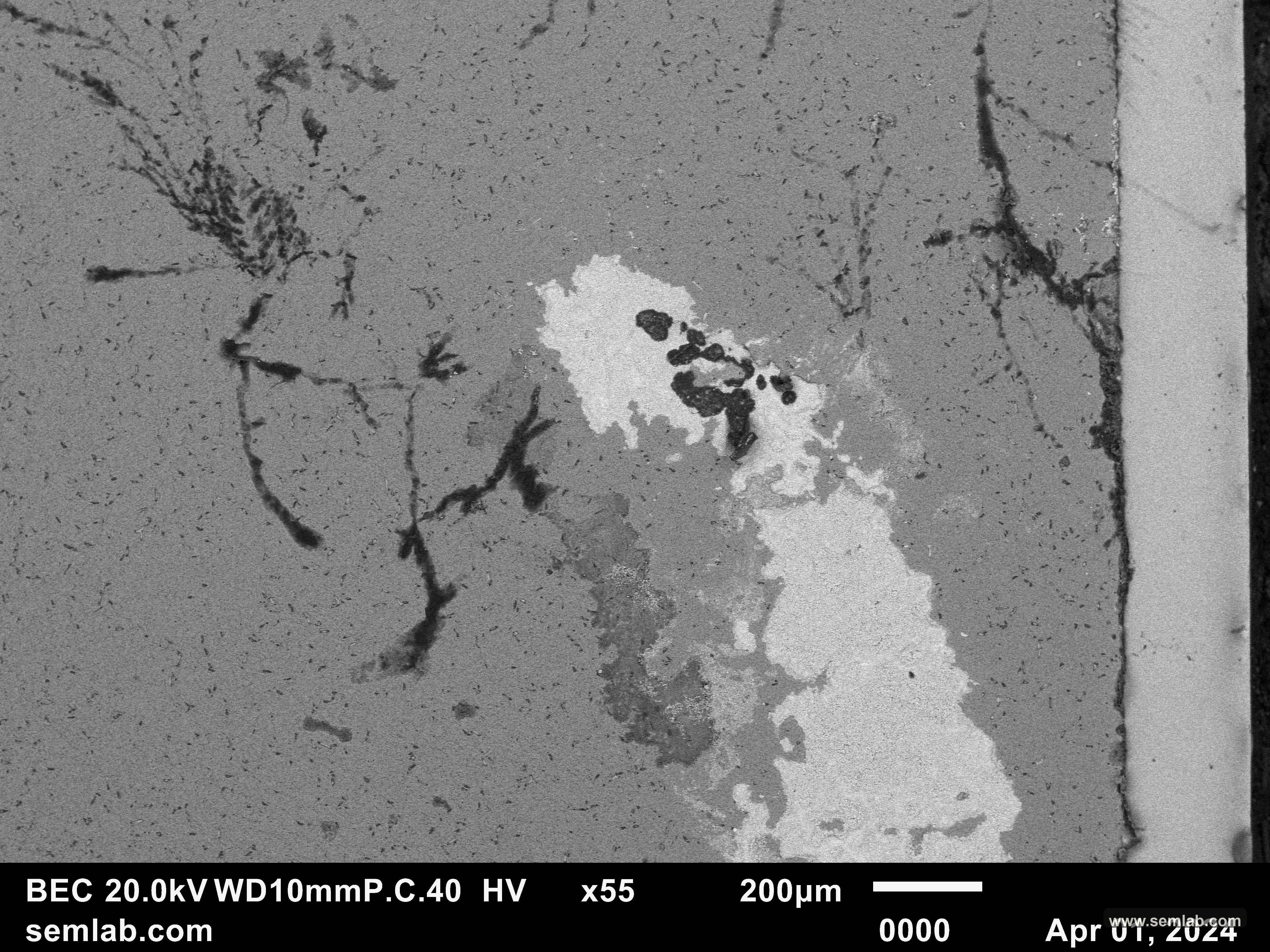
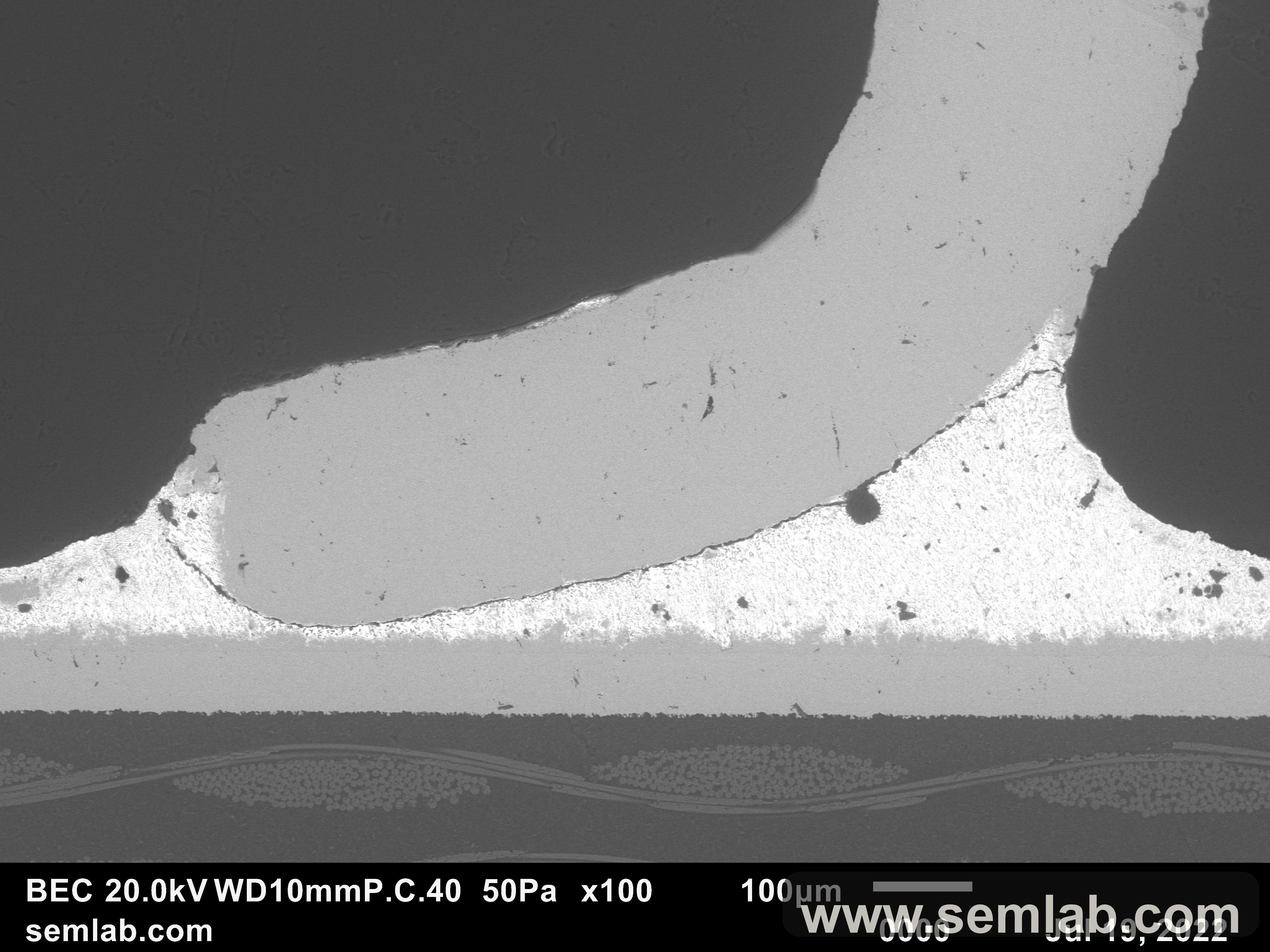
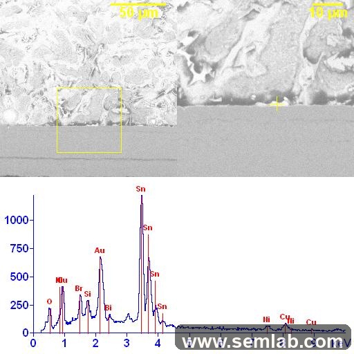
- Primary-site interpretation and comparison examples
Member Image Library
This library groups image-centered examples by mechanism so users can compare what they are seeing to documented patterns in electrical overstress, corrosion, fracture, and delamination.

Each entry connects visible evidence to a likely mechanism, with related notes for deeper failure-analysis context.
Browse By Topic
The library is organized as a curated set of clear reference images rather than a large, hard-to-navigate archive.
Gallery Preview
Selected examples show the kind of physical evidence engineers can compare against their own observations.
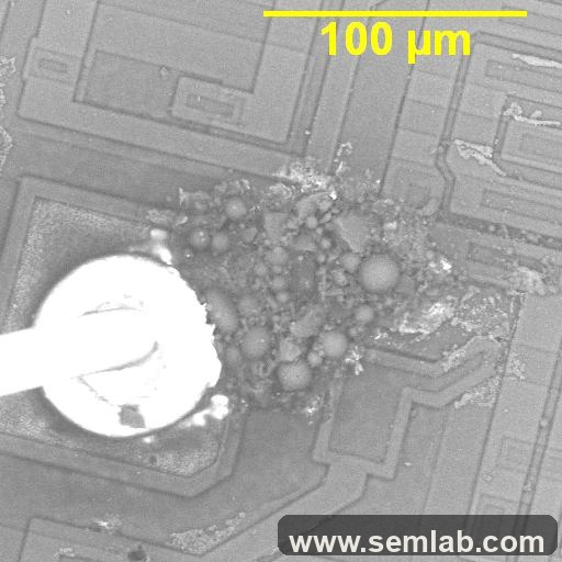
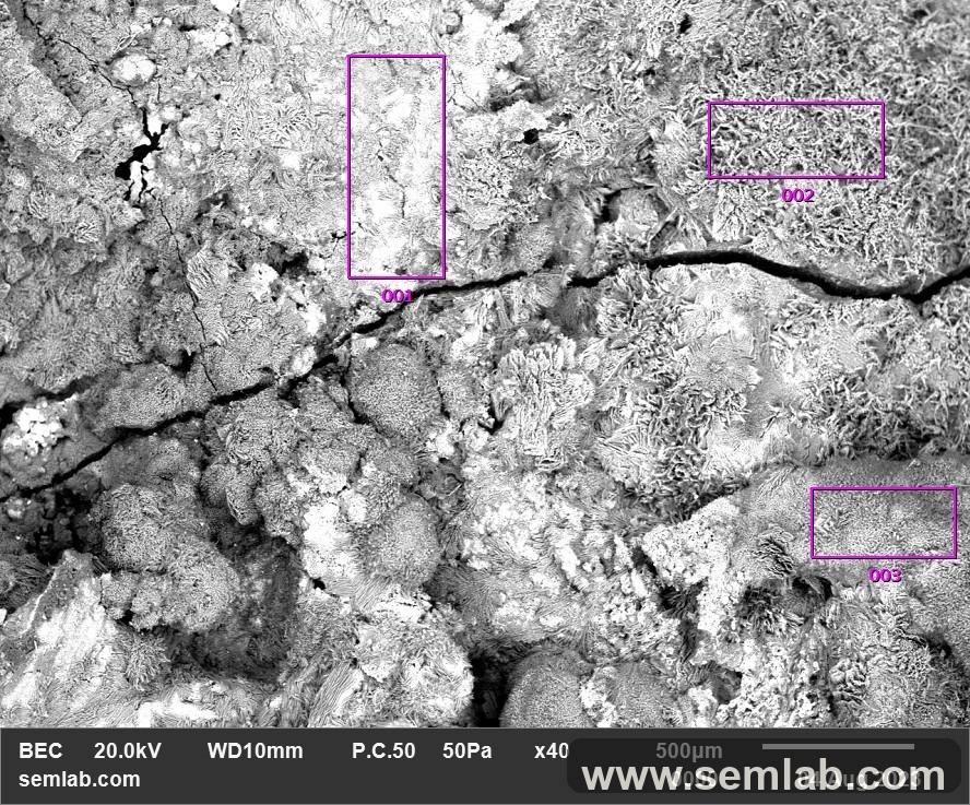
Localized output-region damage with surrounding die geometry still visible.
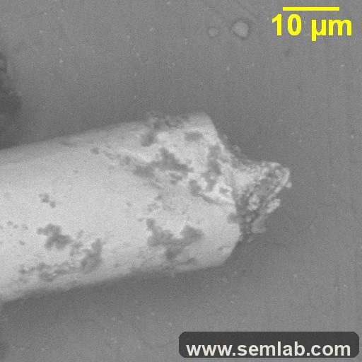
High-magnification wire-fusion example with melt and resolidification evidence.
Localized internal damage that teaches primary-site interpretation rather than aftermath only.
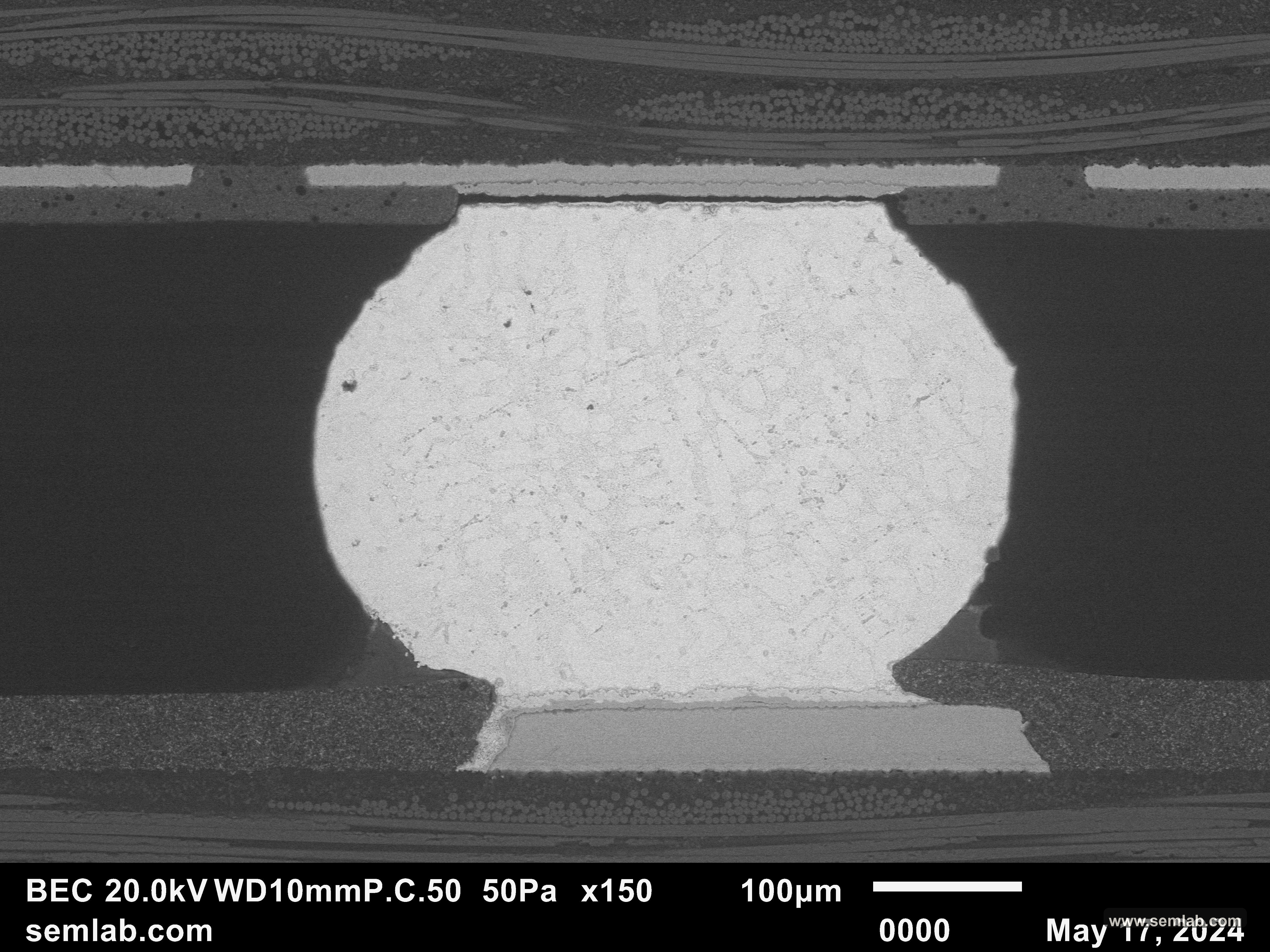
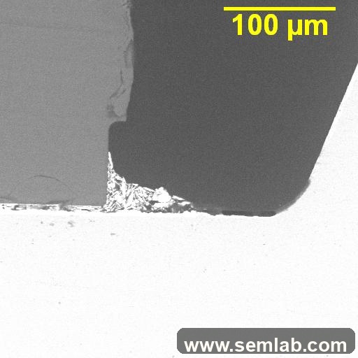
Visibly dramatic damage that is valuable because it was not the initiating failure.
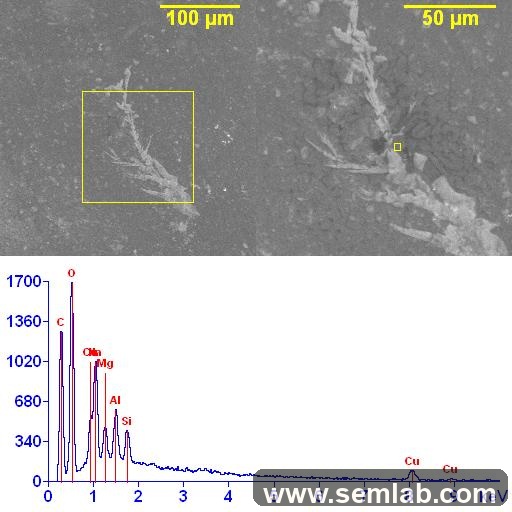
Mechanism-focused corrosion image at a functionally relevant conductive location.
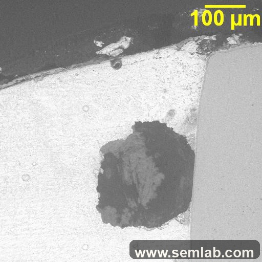
Localized die-surface attack at a functionally important bond-pad region.
Classic electromigration image suitable for leakage and shorting discussions.
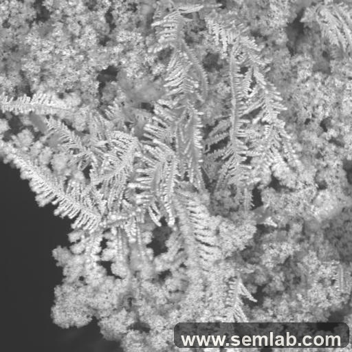
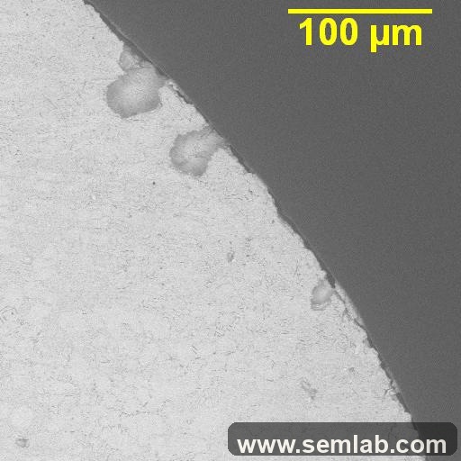
Dendritic growth showing that conformal coating does not eliminate leakage risk.
Geometry-driven leakage example showing why some contamination failures are context dependent.
Acceptable-looking solder joints can be just as important as obvious defects when narrowing the failure mechanism.
Visible residue that should not automatically be overstated as the failure cause.
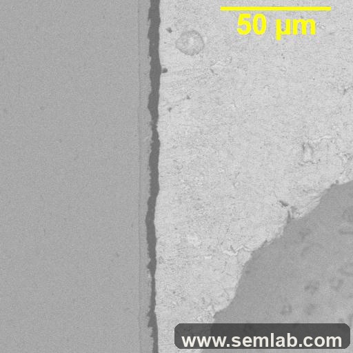
Clear circumferential barrel-crack example tied to multilayer PWB fabrication quality.
Initiation-focused fracture image that helps distinguish origin from broader propagation features.
Internal capacitor crack that directly explains an electrical low-capacitance symptom.
Lead-to-solder interface fracture associated with vibration-driven failure.
Pad-interface fracture image that is distinct from PCB pad cratering and easier to teach cleanly.
Large nearby voids can influence which interface becomes the preferred fracture path.
Clean interface-following fracture without the distractions of a mixed or more complex case.
Board-bending damage at a BGA interconnect with a strong pad-cratering signature.
Clean interface-separation example with a clear, easy-to-identify boundary.
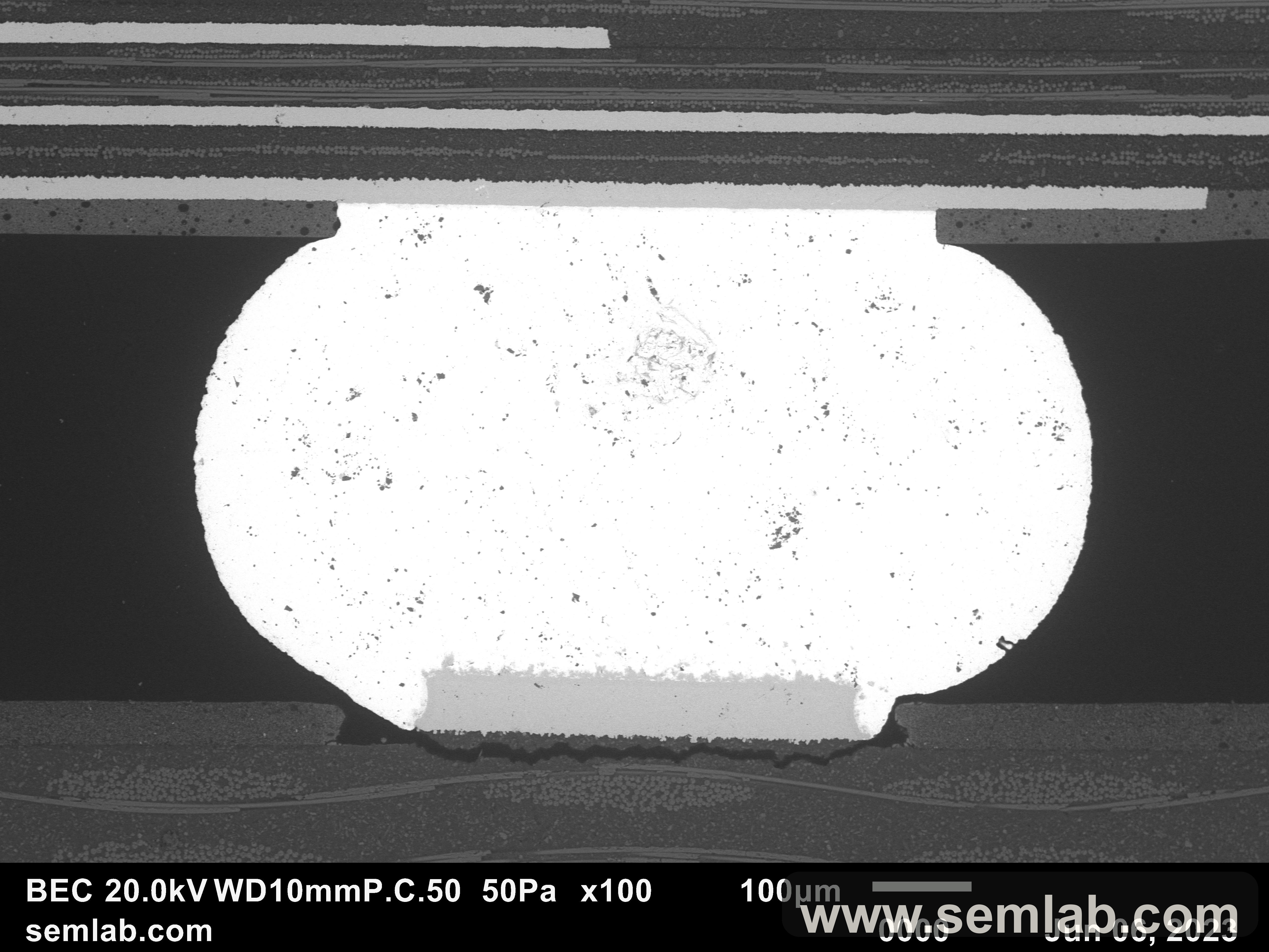
Large solder-joint void at a critical interface rather than dispersed bulk porosity.
Reference for showing that void morphology and location matter more than a simple void percentage.
Combines voiding and residue interpretation in one image instead of treating them as separate questions.
Shows local support loss and stress concentration at a meaningful interface location.
Interfacial-microstructure example because the voiding is concentrated at the interface rather than in random bulk porosity.
The key issue is interfacial development and process adequacy, not a visually dramatic crack or burn site.
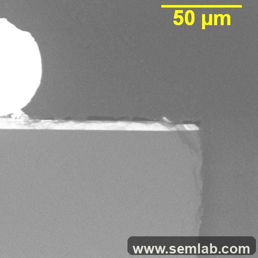
Clear separation image tied to incomplete adhesive fill at the bondline.
Thermally driven interface separation at a different LED-package boundary.
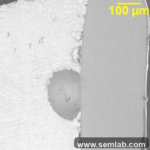
Packaging void tied to local support loss and later die-cracking risk.
Internal package void that may matter because it changes local thermal conditions.
Working Model
The image library is strongest when it helps your team get closer to the right mechanism quickly. When the case still needs judgment, context, and written interpretation, move to a focused SEM Lab review.